Optical Component Design -- Hi Resolution Mask Issues

Steve DiBartolomeo
Applications Manager

Designers of optical components for the telecom industry take advantage of the existing mask and etching infrastructure developed by the IC industry in order to produce their fine geometry structures. However they frequently run into problems that were not anticipated because there are very important differences between optical layouts and IC layouts.

This article describes those differences, how those differences can cause problems in the masks used to define the structures and how one can work around such problems.

Our paper discusses the problems encountered when converting CAD data produced in AutoCAD (or equivalent layout software) which is converted to mask data.

Often there are two conversions -- first from the AutoCAD database into the IC industry standard GDSII stream database -- then into a specific mask making machine data format such as MEBEs. The machine that writes the mask, typically an electron beam writer manufactured by ETEC, reads the MEBEs database.

Characteristics of Optical Structures

Optical structures such as waveguides, couplers and switches are characterized by:

  1. Narrow channels on the order of 1 um

  2. Can be very long - up to 10,000 to 100,000 um

  3. Width or spacing between wall guides changes very gradually

  4. No sharp steps or bends are allowed

  5. Design data is often described using curves or splines.


Waveguides in a Grid Based World

When optical designers hear about the IC industry's ability to image sub micron lines they assume that their structures should also be easy to image. However, some of their requirements don't align with the IC processes. For example:

IC CAD data is grid based. Many years ago the grid value was 1.0 um. It has steadily dropped to 0.5 um, 0.25 um and continued even below that. However in the IC world there is no need to smoothly change the width of a line -- So these tight resolutions may apply only for parallel and very short lines.
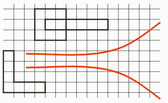
optical waveguide

IC CAD data is never described using arcs or splines. In fact, even most lines are only drawn at 90 degrees. CAD data for optical structures that uses arcs must be reduced into line segments. This can be a major source of errors if the conversion rules and limits are not understood.
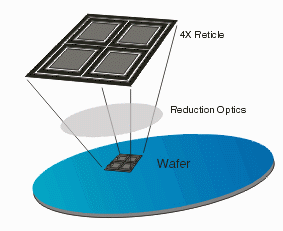


reticle reduction  

One way that IC designers get such fine lines is to use a reduction lens during the imaging process. This means that their masks are actually 4X or 5X the actual line widths imaged on the wafer. It turns out that many optical components cannot be imaged in this fashion -- there is an upper limit to the size of a single die when reduced like this and many optical components exceed this limit. Therefore they must be imaged at 1:1.
Types of Errors

There are quite a few ways that the original design data will be tweaked as we go through the translation from the original CAD data to the mask.

  • Grid Snap Errors

  • arc and spline conversion errors

  • polygon size errors


Grid Snap Errors

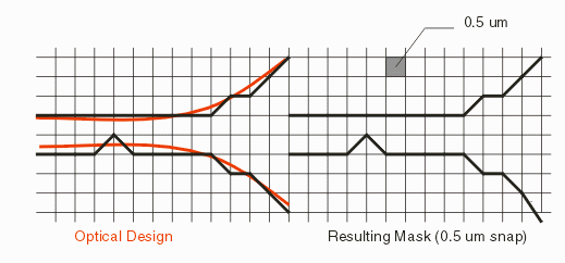
Many designers of optical structures require smoothly tapering edges in order to achieve desired results -- however all IC mask writing and CAD data is grid based. The grid value varies - but if your design depends on data dimensions near the grid size it becomes a very critical factor in the final output. The illustration below shows how a structure that is designed without considering the grid will be modified during data conversion.

grid snapped tapered waveguide

The grid snap errors often don't show up in the first conversion -- from DXF to GDSII. That's because the GDSII output can be set to an impossibly small grid value - 0.001 um. However the next conversion step, to MEBES, will enforce the mask machine's grid snap. This varies from machine to machine but ranges typically in the 0.25 to 0.125 um range. A 0.25 um grid snap can still be noticeable for many optical structures.

Solutions?

One cannot remove the grid snap behavior of the conversion -- but you can modify your design approach to recognize it and to work with the snap -- not against it. First, you must verify with your mask vendor exactly what the value of snap is. Some e-beam machines can run at different grid (also called addressibility) values. Typically the finer grid settings cause the machine to run much slower, so if grid snap is an issue, make sure that your vendor is running the machine at it's best setting.

Second, if you do your own GDSII conversion, you can set the output grid to the same value as the e-beam machine's grid. Then, inspecting the resulting GDSII should show the same snap as the final output.

Third, you can modify your design tools so that you superimpose the grid over your CAD data and modify your data in critical areas so that the snap is controlled. For example, take special care that the two edges of a waveguide are positioned on grid such that they both snap in the same direction at the same time -- otherwise you may see some width discontinuities.


Converting Arcs and Splines

If Optical designers used IC layout tools there would be no conversion from arcs and splines to segments since no arcs or splines are allowed in such tools. In the optics world, a variety of CAD tools are used: sometimes coming from the mechanical design world (AutoCAD, Unigraphics, Solidworks) and sometimes homebrew -- especially some auto-generated layouts whose input is parameters and equations.

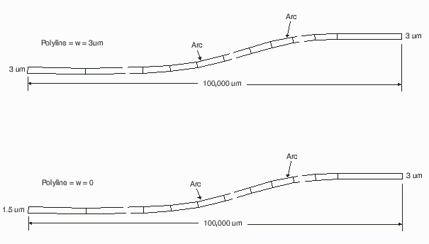
The problem of course, is that since the mask software and tools do not support arcs, the arcs and splines must be fractured or segmented. Obviously there will be some difference between the true arc and the approximation -- but sometimes due to computational shortcuts or assumptions the introduced errors become severe.

Errors in computation are often exaggerated for optical components because the radius of the arc is extremely large.

optical_design2.gif


Configuring the Translator

Improper configuration of the translator is also responsible for avoidable errors. Many errors are introduced when converting units. If the designer is working in units of inches, mils or mm then the data should be scaled during conversion into microns which is standard in the semiconductor industry. However the designer should be sure to have enough accuracy at the input side -- the UM side is generally output at 0.001 um resolution.

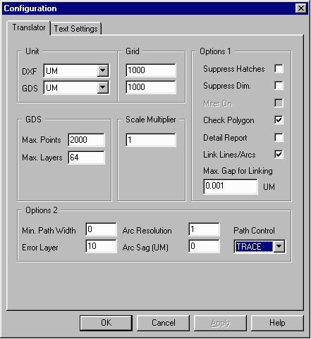
The ASM 3500 DXF2GDS Configuration Menu must be set properly otherwise data will not be translated properly and may look distorted when viewed.

  config_settings.gif


DXF UNITDXF GRIDSCALEGDSII UnitGDSII Grid
inch100000025400um1000
mil10000025.4um1000
mm10000001000um1000
um10001um1000


Other Configuration Settings

MAX POINTS

The original GDSII spec limits the max number of points per polygon to 200. Many mask shops can take now polygons with up to 4000 or 8000 polygons. Consult with your vendor before defining a value. A safe value is 2048.

Chord Error

This will determine the max error between the approximation using segments and the original curve. Less segments are needed for curves of small radius and more segments will be used when the curve radius is large in order to insure a constant known difference. It is difficult to advise what value to set without knowing the application.

MAX LAYERS

Determines the highest layer number allowed in the GDSII file. The standard value is 63. However, many CAD systems support up to 255 layers. You should leave this value at 63 unless you are sure that your target system can accept more. The maximum value you can set is 1024.

LINK LINES / ARCS - MAX GAP

The link line option will link lines/arcs in the DXF file to GDSII boundaries as long as they are connected end to end OR they are within a small gap defined by the user as MAX GAP.

ERROR LAYER

The GDSII file requires all polygons to be closed, were in AutoCAD a designer may leave lines unconnected by accident. When the user defines an error layer (say 20), all open lines/arcs will go to layer 20 in the output GDSII file. When the conversion is done, the user can check layer 20 with our GDSVU and make sure there is no data on that layer.


Special Polygon Chopping Feature in DXF2GDS

Version 6.xx of the DXF2GDS converter can handle complex boundaries drawn by the AutoCAD designer (especially circular traces for waveguides and optical designs) automatically. If a large polygon has more vertices than the upper allowed limit, the software subdivides the large boundary into multiple smaller ones that do not exceed the max vertex limit.


EXAMPLE

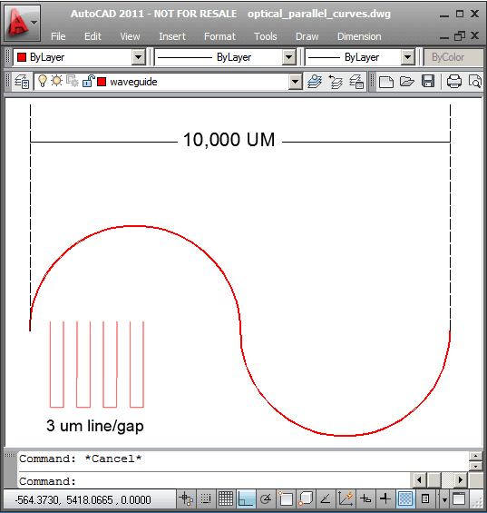
In this example of four parallel curved tracks, each boundary is formed from four large arcs. The arc is 5000 microns, the width is 3 microns and the gap between the curves is 3 microns.

optical_parallel_curves.zip DXF/GDSII Files
(72KB zipped )

  acad_curves.gif
 

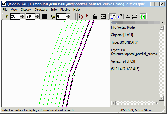
If we translate this to GDSII using an arcres = 9 degrees then the approximation by using a relatively small number of segments is quite noticeable - such sharp bends are unacceptable for optical applications.

  low_res_gdsii.gif
 

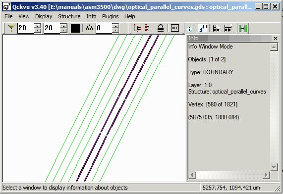
If we translate this to GDSII using a chord error of 0.15 um (which limits the max error between the arc and the approximation to .15 um or about 5% of the line width) then the approximation is quite good. However now we have more than 1800 vertices per boundary.

  high_res_gdsii.gif
 

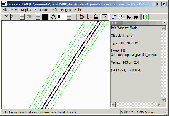
If we need to have a very high resolution but keep our vertex count per boundary low, we set the max vertex=256 and the chord error=0.15 um. We get the same smooth output but we won't get any boundaries with more than 256 vertices and there is no manual CAD work to do.

  high_res_gdsii_w_max256.gif