
Artwork developed the "die clean" module or polygon filter in response to a problem posed by one of our package design customers. The IC designer had sent him the top metal layer in GDSII format and expected our package designer to extract out the pad coordinates from that layer.
The problem here is one of magnitude. The top metal layer is enormous and when the package designer attempted to do a straight conversion to AutoCAD (where he could digitize the pad centers) he got a 1000 MB DXF file -- too large to open.
What our package designer friend wanted, and what we provided, was a GDSII filter that could quickly check each polygon and filter it out based on its size and shape. By properly setting up some rules that would pass only the die pads and remove everything else, he was able to get a tiny (2KB) GDSII file that was easy to deal with.
After you have started GDSFILT, loaded the desired GDSII file and selected just the layer(s) you want in your output file, return to the main menu and check the button marked Polygon Filtering. Then press the button to enter the polygon filter dialog.
Note: the polygon filter is not a part of the standard GDSFILT release and requires an additional license. If the check box does not cause the button to light up then the license is not in place.
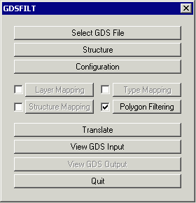
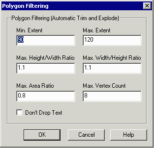
There are several settings used to filter out polygons. A polygon only passes to the output if it passes all of the filter tests.
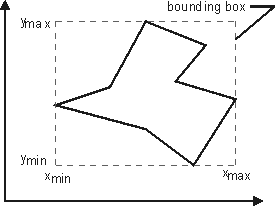
The polygon filter first calculates a bounding box for each boundary or path. This is the rectangle (or square) that just surrounds it. The bounding box is used instead of the actual polygon for most of the tests (not for area ratio) -- this makes the testing very fast when you thousands and thousands of polygons to evaluate
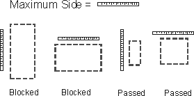
Designed to eliminate all polygons that are "too big". Specify a maximum side and any polygon whose bounding box maximum side exceeds your limit is blocked. All other polygons are passed. For example if you want to get die pads that are 80 um square set your max side to something slightly larger than 80 um.
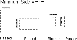
This test is designed to eliminate all polygons that are "too small" such as vias and contacts. Specify a minimum value and any polygon whose bounding box minimum side is smaller than your setting is blocked. All other polygons are passed. For example if you want to get die pads that are 80 um square set your min side to 75 um and all contacts and vias (which are square but which are very small) will be filtered out.
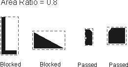
Designed to eliminate all polygons that don't "fill" their bounding box. The area covered by the polygon is divided by the area of the bounding box. Items such as rectangles and squares have a 1.0 ratio. A die pad with a chamfer will have a .85 to .95 ratio. L and C shaped polygons tend to have a low area ratio.
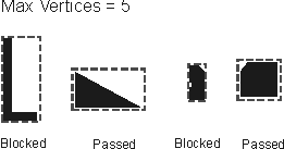
Designed to eliminate all polygons that are too complex. Typically your die pads have 4 to 6 vertices - rectangles have 4, a corner chamfered rectangle has 5 and two chamfers have 6 vertices. Any polygon whose vertex count exceeds your setting will be eliminated.
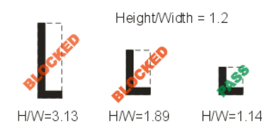
This test is designed to eliminate all polygons that are too tall. Not only is this good for isolating pads, it can be used to isolate horizontal traces. Typically, die pads have a height/width ratio near 1.0. By setting a value such as 1.2 you will eliminate any polygon whose height to width ratio (bounding box) is greater than 1.2.
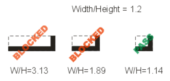
This test is designed to eliminate all polygons that are too "wide". Not only is this useful for isolating die pads, it can be used to isolate vertical traces. Typically, die pads have a width ratio near 1.0. By setting a value such as 0.95 you will eliminate any polygon whose width to height ratio (bounding box) is less than 0.95.
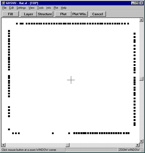
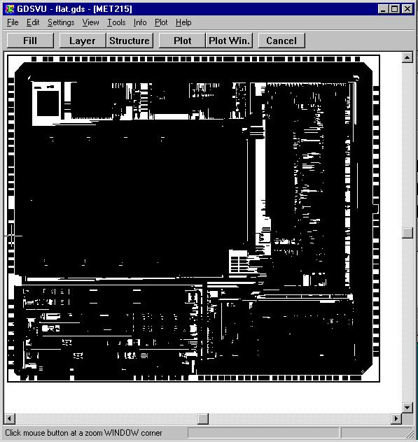
To illustrate the usefullness of the polygon filter, we ran a 96 MB GDSII file generated by the chip designer who exported only the top metal layer. The package designer needed to extract out the pads to produce his bond wire document. The data was too large to translate directly into to AutoCAD; the resulting DXF file would have been > 2 GB. There are about 124,000 boundaries/paths in this M1 layer; the package designer only needs to pull out the 136 die pads that lie around the periphery of the chip.
The chip's top metal layer is so dense that you cannot see individual lines or pads.
We ran the above file through GDSFILT's polygon filter with the intent of identifying the die pads only and removing anything that wasn't a die pad. Filter parameters used to isolate the 75 um square die pads were:
Max Extent: 80
Min Extent: 70
Max H/W Ratio: 1.05
Max W/H Ratio: 1.05
Max Vertex: 6
Max Area Ration: 0.95
