

For wafer level packaging one may need to create masks that are "smooth" at the edge of the wafer in order to control the rate of conductor etching or plating. If the circuitry terminates abruptly, the change in metal density can negatively effect the uniformity of plating and etching.
To achieve the smooth edge, we step the circuits out past the desired border and then use HExtract to trim them to a circular boundary.
The design at right contains about 7200 2.2 x 2.2 mm RDL circuits arrayed on a 200 mm wafer.
The GDSII file is quite small since it consists of a single circuit and a large number of SREFs.
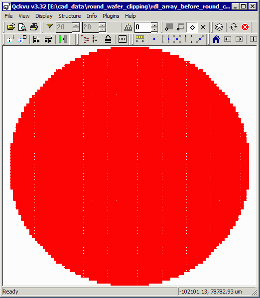
In this design we've stepped the circuits out to the 100 mm radius of the wafer but then we will trim back to a 94 mm radius. The metalization beyond the 94 mm radius has the same density as the good chips and will insure that the good chips on the periphery are uniformly plated.
Turn on layers that you wish to extract. Start the HExtract by clicking on the Plugins menu and selecting HExtract. The dialog will pop open.
Clip Data - select this so that the data is clipped to the window edge.
Generate Flat Output - don't select this as it would flatten the entire output and make the GDSII file very large.
Circular Window - select this option for clipping your wafer.
Center - enter 0,0 (assuming this is how your wafer data is centered ...)
Radius - enter 94000 as this defines the edge we wish to clip to ...
Arc Res - this parameter controls the smoothness but since we are going to rely on Chord Error we set it large.
Chord Error - by setting this to 2 (um) we insure that the circular window is very smooth and does not deviate more than 2 um from a perfect circle.
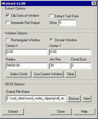
Once you have set all the parameters, select the name of the file you wish to create. Then click on Extract. The processing may take anywhere from 10 seconds to 60 seconds depending on the complexity of your data and the speed of your machine. While the program is running you cannot close the dialog or do any action in Qckvu3.
Once complete, you can use the View button to open a the output file (only if you have enough Qckvu3 licenses ... otherwise you will need to close the source file first ...)
Let's examine the results of this clipping.
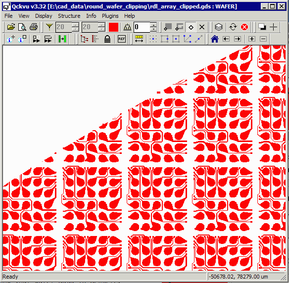
The smooth clipping edge is clearly apparent.
However upon closer examination one can see tiny slivers - very small pieces of conductor due to the cutting edge passing through most of a pad or trace.
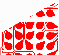
It is usually good practice to remove these small slivers. In order to do that automatically, HExtract has a sliver control parameter.
The sliver parameter actually examines the ratio of the perimeter to the area of each polygon left after clipping and deletes ones that are smaller than the parameter value. Below is shown the effect of various sliver parameter values. For reference, the bump pads are 270 um in diameter and the trace widths are 20um (signal) and 50 um (power) in width.
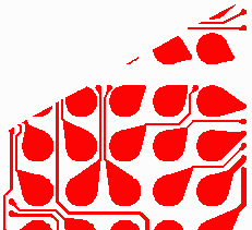
Sliver=10um.
Does not remove any slivers.

Sliver=20um.
The smaller pieces are removed.

Sliver=40um.
All slivers removed.