Antipad in ANF Padstack
Artwork recently completed an ODB++ to ANF converter. Since most PCB tools output ODB++ this becomes a good way to pass layout and net information from PCB tools that do not have direct Ansoft interfaces.
ODB++ can contain a lot more useful information than Gerber/Drill.
For example, a well written ODB++ file will contain an EDA section that includes component placement and pin information and netlist information. All of this data can be then passed intelligently to Ansoft simulation tools via the ANF file format.
Padstacks
While ODB++ does not make explicit use of padstacks, we have developed an algorithm that examines the pads associated with drill holes and can build padstack libraries. We start with a simple ODB++ file for a 4 layer PCB. The two inner layers are for power and ground.
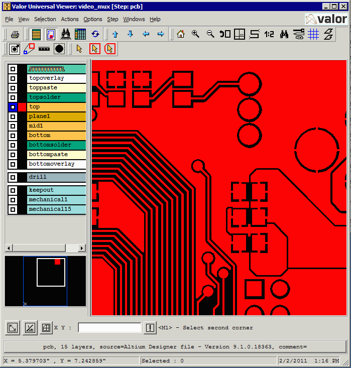
We then attempt to transfer these padstacks into ANF (2.0).
Passing Through Power and Ground Planes
This process works well until we get to a situation where we have power and ground planes. The pad that is located on a power or ground plane is generally of three different types: a) a null pad (i.e. one where the via connects to the plane), a thermal relief (i.e. one where the connection to the plane has some small cutouts to reduce thermal conductivity) and a clearance (one where some of the ground plane metal is removed or cleared away to allow the via to pass through unconnected.)
Here is a 3D Example (Artwork's 3DVU) of a signal passing through the two middle layers which are power and ground planes:
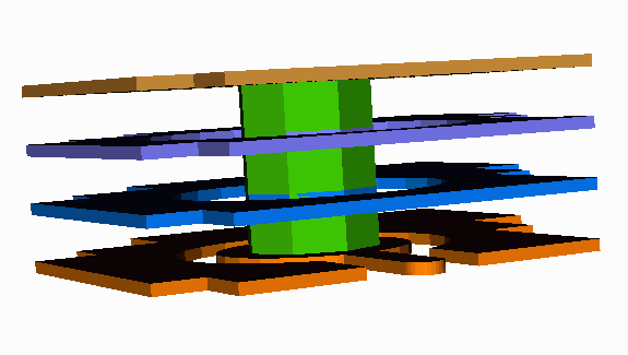
You can see the "clearance" holes through the plane layers easier if the top and bottom layers are turned off.
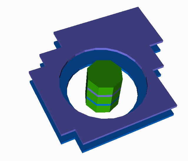
The standard method of creating such pad stacks is to define a pad on each layer. For clearances in a ground/power plane, the pad is defined as a hole or "antipad."
However when we examine the Ansoft ANF specification we do not see any syntax describing how to create a antipad (or negative pad)
Here is the padstack definition in Artwork's internal ASCII format:
29    padstack_29
B_PADSTACK_GEOM
1     C 0.040000     0.040000     0.028000     P
2     C 0.028000     0.028000     0.028000     P
3     C 0.068000     0.068000     0.028000     N  <--- the N indicates a antipad (on M2)
4     C 0.028000     0.028000     0.028000     P
5     C 0.028000     0.028000     0.028000     P  <--- why is this P?
6     C 0.028000     0.028000     0.028000     P
7     C 0.040000     0.040000     0.028000     P
E_PADSTACK_GEOM
What I found curious was that there is only an antipad on stackup 3 (M2) and none on stackup 5 (M3). Why? It turns out that if you examine the ODB++ file directly, you will find that M2 is a negatively drawn power plane and M3 is a positively drawn power plane.
Now here is the ANF padstack that we create:
29  padstack_29
    B_PADSTACK_GEOM
      1    E  0.04     0.04     0.028
      2    E  0.028    0.028    0.028
      3    E  0.068    0.068    0.028  <--- how do we indicate this is an antipad?
      4    E  0.028    0.028    0.028
      5    E  0.04     0.04     0.028
      6    E  0.028    0.028    0.028
      7    E  0.04     0.04     0.028
    E_PADSTACK_GEOM
What Ansoft Links Shows
If you open our ANF file in Ansoft Links and examine each layer separately you will see:
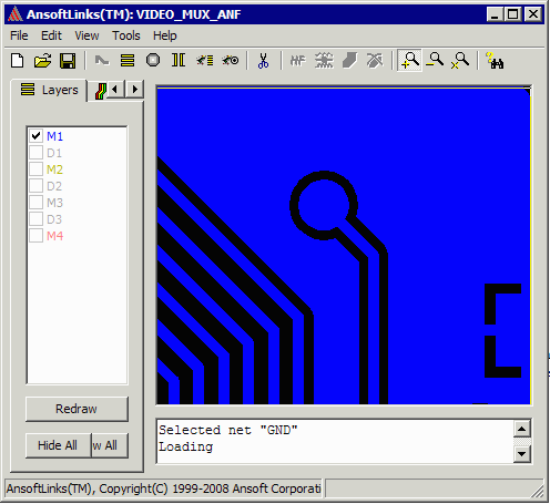
The top metal layer looks fine. (Expected)
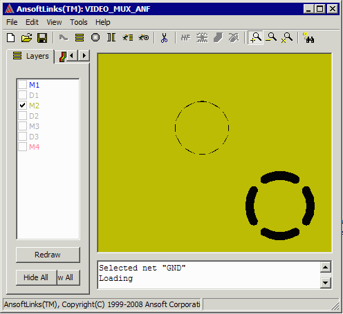
The ground plane layer (reversal) is shorted due to lack of a antipad definition.
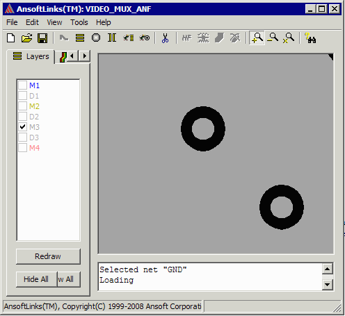
The power plane layer (positive) is OK.
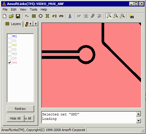
The bottom layer is OK. (Expected)
You can see that our internal padstack format is almost identical to ANF's. However Artwork has an additional column P/N that indicates whether the pad shape is positive or negative. The N allows us to convert the pad into a "cutout"
So our question is: HOW DO WE DEFINE AN ANTIPAD in ANF 2.0?