
 |
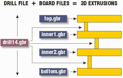
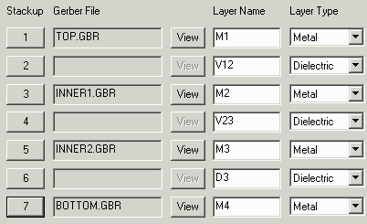
Processing Non-Stackup Layers into 3DNetex-G and Netex-ODB were originally designed to server the EM simulation discipline -- because of this only the conductor and drill layers that define the stackup are described in the main dialog. |
||
 |
 |
|
|
For 3D mechanical modeling there are additional layers and functions that need to be addressed. a) we need a way to define the board's outline (or profile as it is known in ODB++ parlance.) b) we need a way to define any cutouts (or routs) that are machined into the board. c) we would like in some cases to add other layers to the top and bottom of the stackup - in particular the solder mask and a silkscreen. Since these other layers are not really a part of the stackup we decided to create a new dialog box that would give us some flexibility in loading them and defining their behavior. We call this the Other Files dialog and it looks like this: 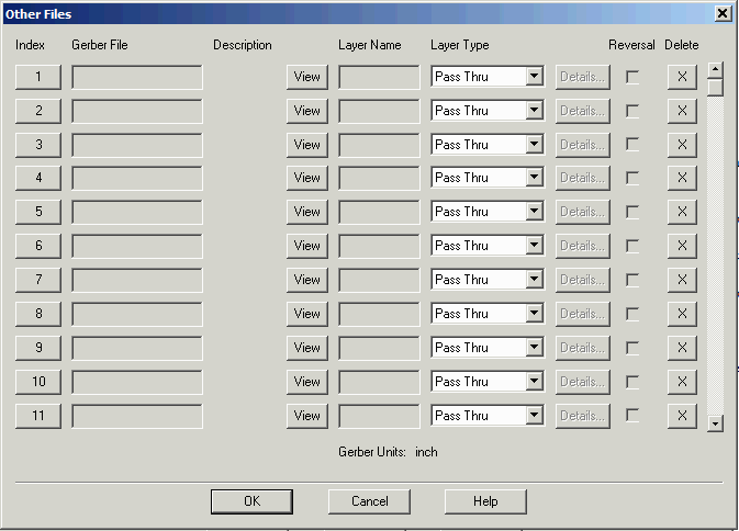
Details Index - is merely a number for keeping track of these files. Click on the button to open a dialog that will enable the user to pick a Gerber file. Gerber File - this is the data file (whether it comes from ODB++ or direct) to be loaded and processed. Layer Type - this tells the program what to do with this data. There are the following types available: Profile - defines the profile or outline of the board. Anything outside this profile is clipped away. an ODB++ file should always come with a profile. For Gerber input, use or create a layer that has a single closed contour that defines the board's outline. 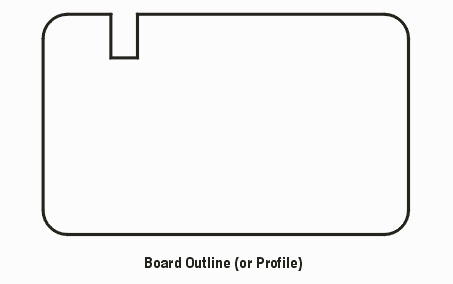
Rout - similar to a profile but often includes traces with width inside of the board. This can be use to remove or rout out regions throughout the board. The rout data is considered to go through all metal and substrate layers and solder masks and silkscreens. 
Btm Soldermask - used to build a soldermask extrusion on the bottom of the board. Top Soldermask - used to create a soldermask extrusion on the top side of the board. Btm Silkscreen - used to create a silkscreen extrusion on the bottom side of the board. If there is a solder mask it goes between the bottom conductor and the silkscreen. Top Silkscreen - used to create a silkscreen extrusion on the top side of the board. If there is a solder mask it goes between the top conductor and the silkscreen. Pass Through - has no function for 3D output. (It is there for DXF and GDSII output) Reversal - solder mask layers are often drawn as reversals. Make sure to check this option if the solder mask is drawn as a reversal. 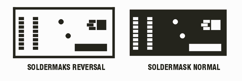
|