
 |
|
Back Drilling Backdrilling is a manufacturing technique used on high speed multi-layered boards to reduce the amount of parasitics generated by plated through holes. We encounter it mostly on designs where the bit rates are 10GB and above and where there are 12 or more layers. Backdrilling is used because it is expensive to manufacture boards with buried and blind vias. Additional drilling and lamination steps are required when you have buried and blind vias. But using through hole vias when one is not moving a signal from the very top to the very bottom of the board generates a new problem - the unused "stub" section can act as a tiny antenna and couple to other traces. While this effect is not a problem at low frequencies, the higher the frequency, the more significant the stub becomes. |
||
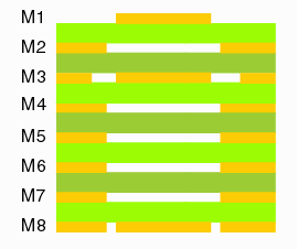
| Laminated; Not Drilled After the individual double sided boards have been etched they are laminated under pressure and temperature; they will then be sent to the drilling station. In this crossection, our objective is to move a signal from M1 to M3 using a via. You can see metalization for a pad on layers M1, M3 and on the bottom (M8) |
 |
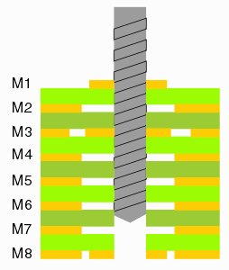
| Drilled A drill goes through the entire substrate. This provides a cylindrical hole that will be plated with metal to make the connection between conductor layers.
|
 |
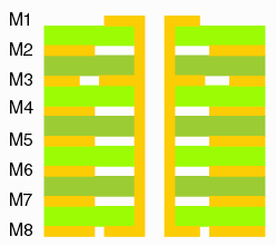
| Plating After some chemical etching to prepare the surface the board is dropped into a plating solution. Copper is deposited in the cylindrical hole producing a connection from top to bottom and to any layers that were metallized in the are of the hole.
|
 |
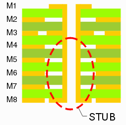
| Unwanted Stub Our signal only needs to go from M1 to M3. But you can clearly see that we have a "stub" that extends from M3 all the way to M8. This can couple to other signals; even if there are not other signals to couple to, the stub couples to the ground planes and acts as a capacitor.
|
 |
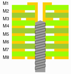
| Back Drill A partial solution is to flip the board over after plating and drill from the rear through the plated through hole. The diameter of the back drill is large enough to remove the copper from the via. [you can also drill from the front for signals that go from M8 to M6 -- nevertheless we'll stick to the terminology backdrill.] |
 |
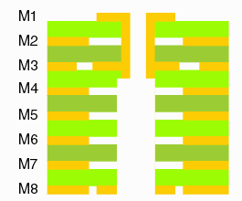
| Final Result After the backdrill is complete you can see that the via from M1 to M3 does not extend down to the bottom of the board; the capacitive coupling and antenna radiation are eliminated.
|
 |
Simulating Back Drilled BoardsIf you are using an advanced EM simulator to predict impedance, coupling or delay and you are working at bit rates or frequencies of 10GB/10GHz and above then you will want to take the back drilling into consideration. Problem - ODB++ Doesn't Know About Back Drilling Unfortunately, the ODB++ database does not have a way to mark drill data as back drilling. Such drill files will appear in the ODB++ database but our program has no automatic way to determine that they are in fact back drills. We have enabled a user option in the program (Expect Back Drill) that when turned "on" will check the drill files to see if they share common coordinates that pass through common layers. Under this condition it can detect back drills and will modify the output vias accordingly. |