 |
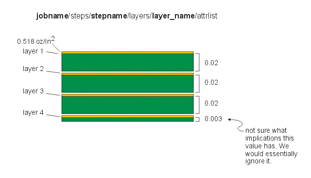
Substrate PropertiesSeptember 3, 2013 Steve DiBartolomeo Artwork was recently advised by Mentor Graphics that the Expedition PCB design and layout software now utilizes two layer attributes that can be read and used to pass substrate thickness to other programs such as EM simulators. Where to find the attributes? In ODB++'s hierarchy there are layer directories that contain the "features" used to render each of the conductor layers. Each layer directory can have an attribute file asssociated with it. Expedition is now writing two useful attributes for each layer:jobname/steps/stepname/layers/layer_name/attrlist A sample attrlist file for layers 1-4 contained: |
.cu_base=NO .eda_layers=layer_1 .inp_file= .lpol_done=NO .out_angle=0.0 .out_comp=0 .out_mirror=NO .out_polarity=Positive .out_x_scale=1 .out_y_scale=1 .comment=layer_1 .layer_dielectric=0.02 .layer_hdi_type=Core .copper_weight=0.518917 |
.cu_base=NO .eda_layers=layer_2 .inp_file= .lpol_done=NO .out_angle=0.0 .out_comp=0 .out_mirror=NO .out_polarity=Positive .out_x_scale=1 .out_y_scale=1 .comment=layer_2 .layer_dielectric=0.02 .layer_hdi_type=Core .copper_weight=0.518917 |
.cu_base=NO .eda_layers=layer_3 .inp_file= .lpol_done=NO .out_angle=0.0 .out_comp=0 .out_mirror=NO .out_polarity=Positive .out_x_scale=1 .out_y_scale=1 .comment=layer_3 .layer_dielectric=0.02 .layer_hdi_type=Core .copper_weight=0.518917 |
.cu_base=NO .eda_layers=layer_4 .inp_file= .lpol_done=NO .out_angle=0.0 .out_comp=0 .out_mirror=NO .out_polarity=Positive .out_x_scale=1 .out_y_scale=1 .comment=layer_4 .layer_dielectric=0.003 .layer_hdi_type=Core .copper_weight=0.518917 |
|
If you are building a stackup for another program from this information you can use the copper_weight attribute to compute the copper thickness. In the example above all "foils" have a copper weight of 0.519 oz/square foot which is the equivalent of approximately 1/2 mil in thickness. Later releases of the ODB++ (8.1 and later) specification support units other than Imperial. For UNIT=MM then the copper weightThe thickness of the dielectric below each layer foil is specified. The only value that makes little sense is the one assigned to layer 4 which we would assume should be the bottom of the board and therefore has no dielectric below it.  We are also not sure whether we need to address two other attributes: cu_base and layer_hdi_type. Default Values Sometimes an ODB++ file will not include values (or set them = 0) for the copper_weight and the layer_dielectric parameters. Since we can't produce 3D data without some finite values the NETEX-G program will default as follows: Electrical Properties Note that there is no information about the actual electrical properties such as dielectric constant or loss tangent, conductivity and permeability. |