[BGA]
This section allows the user to define parameters of the BGA package; the AIF reader will be able to draw the ball pads and package outline.
Many times a die designer will know the signal name and even the ball assignment for his die pads but does not have the "coordinates" of the ball pads. However often he needs to explore different package options - package size, pitch, ball diameter ...
the [BGA] section in the AIF file allows him to quickly define a package from well known parameters; AIFVU will then draw the package footprint along with the die. This allows the die designer both to see the die together with the package and also to see a ratsnest from die pad to ball pad (assuming nets have been defined.)
Syntax
[BGA]
NAME=BGA                 name (ref designator)
WIDTH=23000              package outline width in same units as  AIF file
HEIGHT=23000             package outline height (y)
PITCH=1270               center-center spacing between ball pads
CHAMFER=UR 250           chamfer on the outline. You can specify all 4 corners
POPULATION= 17 17        number of balls along x and y
DEPOPULATION= 9 9        remove this many balls in the interior
REPOPULATION= 0 0        add back in this many balls (typically ground)
BALL=CIRCLE 750          ball pad shape and size
A1=UL                    location of A1 (looking from above the package)
![[BGA] Section Layout [BGA] Section Layout](/package/aifvu/arraygen_layout.gif)
Notes:
If population is even; depopulation and repopulation should be even. If population is odd, depopulation and repopulation should be odd.
rectangular packages are supported - but pitch must be equal in both directions.
the package outline can have up to four chamfers - UR 1000 LL 500 UL 250 LR 600
New BGA Polygonal Outline
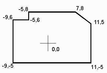
[added 04/26/04]In order to support more complicated packages (in this case a module containing two chips with an irregular outline) we have added a new parameter to the BGA section called:
OUTLINE=POLYGON
with the following syntax:
OUTLINE=POLYGON <num_pgons> <width> <num_pts> x0 y0 x1 y1 ... xn yn
Example

[BGA]
OUTLINE=POLYGON  1  0.1  7   -9 -5  11 -5  11 5  7 8  -5 8  -5 6  -9 6
