Starting Point 2D Drawing
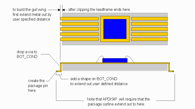
Our starting point is the 2D leadframe drawing. A polygon defines the package body outline and we clip the leadframe conductors to the extents of this polygon. We have already assigned a thickness (T) to the top metal layer and this same thickness is generally used to define the package lead. The lead width comes from the 2D width as drawn.
The package connection to the PCB is approximated by first extending out from the edge of the package boundary, then dropping down vertically (we can't use an angle here as the target CAD systems don't support that type of via) and then out again to the pin.

Because we have to convert this gull wing to a representation in Cadence APD/SIP it is necessary that the drop down of the gull wing be locked to the dielectric thickness defined between the TOP_COND and the BOT_COND.

