Identifying a SIP 3Di File
3Di files generated by SIP normally include some comment lines at the beginning identifying them as coming from SIP.
#######################################################
# File format    : 3Di v1.700000
# Source database: C:/temp/xxxx/yyyy_test.sip
# Generated by   : Cadence SiP Layout XL
#                  S021 16.6
# Date/Time      : Fri Feb 07 09:32:18 2014
#######################################################
Tables
The latest Artwork 3Di files (as of 6/2016) have more tables of attributes than those generated by Cadence. Not all of these tables are related to STEP output but two of them are.
Cadence Tables      Artwork Tables               Comment
TABLE COLOR          TABLE COLOR
TABLE OBJECT         TABLE OBJECT
TABLE LAYER          TABLE LAYER
TABLE NET            TABLE NET
                     TABLE LAYER_TYPE             needed for proper STEP
                     TABLE NET_PINS               useful but not needed for STEP
                     TABLE_STACKUP                we have to build the stackup by scanning geometry data
So there are two additional tables that we really need to create a proper STEP output. The TABLE_STACKUP defines the conductor and dielectric layer order and thicknesses. The LAYER_TYPE is used to identify the dielectrics vs. conductors.
Building a Stackup by Scanning Geometries
Since no explicit stackup table is generated by SIP (though it would be easy to do), we have to scan the geometry data. First, we figure out which "layers" represent our conductors. We do that by scanning the geometry section and checking for net attributes - any geometry with a net attribute must be a conductor. This enables us to determine which SIP layer names are conductors.
GEOM
ID 298641520
OBJECT 7
LAYER 4
COLOR 1
NET 71
EXTR 1 234.000000 254.000000
2DPG 19
-3780.918000 -5099.062000 -3820.674000 -5099.710000 -3822.349000 -5076.096000 -3846.951000 -5006.224000
-3903.763000 -4958.686000 -3922.464000 -4943.872000 -3932.172000 -4922.080000 -3930.677000 -4898.269000
-3918.319000 -4877.862000 -3474.530000 -4434.072000 -3187.633000 -4434.072000 -3179.491000 -4422.934000
-3151.658000 -4395.100000 -3119.700000 -4395.100000 -3041.578000 -4473.222000 -3087.477000 -4519.121000
-3222.700000 -4619.100000 -3247.799000 -4642.898000 -3324.754000 -4642.898000
Since this geometry has a NET attribute it must be a conductor. We can conclude that the layer with index=4 is a conductor layer. By examining the layer table we see that layer 4 = M1.
We then examine these geometries' Z heights -- assuming that all geometries on a given conductor layer share common Z values. Using that information we can sort their layers by position and we can also figure out where the dielectrics fit between conductor layers. We also examine geometries whose Z values fit between conductor layers and can assign those as drills.
Computing Dielectric Extents
You can't automatically determine the X,Y extents of the dielectric just by examining the conductor layers. Fortunately, SIP always outputs a layer called OUTLINE that defines the package outline. We can take that outline and use it as our dielectric extents.
#######################################################
TABLE LAYER
#######################################################

1 WIRE2
2 WIRE1
3 DIE
4 M1
5 M1_P1
6 P1
7 P1_P2
8 P2
9 P2_M2
10 M2
11 VIA DRILL HOLES
12 SOLDERMASK_TOP
13 SOLDERMASK_BOTTOM
14 OUTLINE
15 RATSNEST LINES
Now that we know layer 14 is our outline we search the geometry section:
GEOM
ID 242532264
OBJECT 7
LAYER 14
COLOR 196
EXTR 1 127.000000 127.000000
2DPG 4
-7500.000000 7500.000000 7500.000000 7500.000000 7500.000000 -7500.000000 -7500.000000 -7500.000000
Special Via Layer in SIP
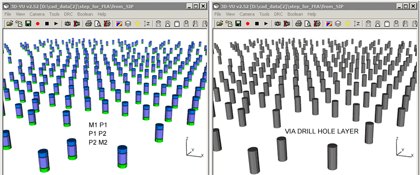
SIP does output a "special" layer that is very helpful for generating STEP. The layer is called: VIA DRILL HOLES and it is an extruded circle that runs from the top of the via to the bottom with no breaks by layer. We can use this layer an no longer need to identify pad stacks in order to build proper via cylinders in STEP.

Separating Solder Bumps from Conductor Layers
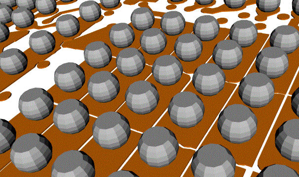
For reasons we don't entirely understand, SIP assigns the same LAYER attribute to the solder bumps as it does to the bottom conductor layer that they sit upon.

SIP output with Layer M2 turned on.
This would result in the solder bumps ending up in the same "part" or "component" in the 3D STEP file; something most users would not want.
We modify this by scanning the bumps based on their OBJECT type and creating a new layer just for the solder bumps.
Unionization of Overlapping Conductor Geometries
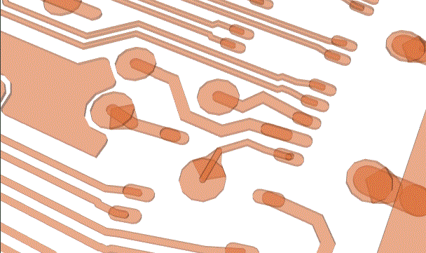
SIP exports each trace, shape and pad independently to 3Di. There is nothing wrong with this but interference between solid bodies is generally not acceptable for FEA style analysis.
This is easily seen by using the viewer's transparency setting on a conductor layer. The "darker" regions are where two solid bodies interfere.

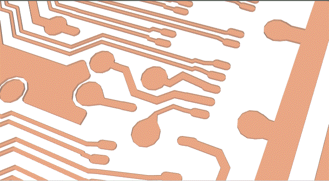
So 3DVU performs a boolean on the conductor layers which combines overlapping traces, shapes and pads. You can see the result below with the same transparency applied:

All of these changes are written to the 3Di database - the user can save the modified database to a new name.
Then our STEP for FEA converter can operate on the SIP 3Di data as if it were generated by Artwork's 3Di writer.
