Differences between Cadence Allegro Native STEP output and Artwork's STEP Output
May 2016
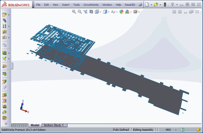
In Allegro v16.6 Cadence added the ability to export a STEP 3D model for the etch classes. While this seemed a very good option for FEA simulation engineers, Allegro board designers have reported that the resulting output is not really useful for FEA purposes.
Let's run through a small example - we'll output STEP directly from Allegro and import it into SolidWorks; We will then output Artwork's 3Di from the same .brd file and convert it into STEP using Artwork 3Di2STEP (optimized for FEA.)
Exporting STEP Natively from Allegro
We'll start with a multi-layer PCB layout (we've removed a lot of the geometries to keep things from getting too big)
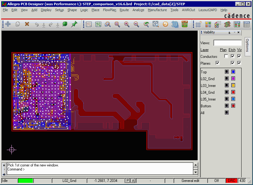
We'll then use the File | Export | Step menu pick to open the Step Export dialog:
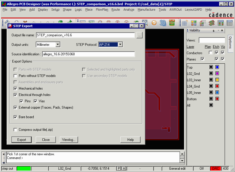
We are interested in getting out the conductor layers (etch/pin/via) and the vias connecting each layer.
Clicking on Export produces a STEP file very quickly.
Exporting 3Di to Get to STEP
In order to export 3Di we have installed Artwork's AWROut plug-in. We start the program and see the dialog.
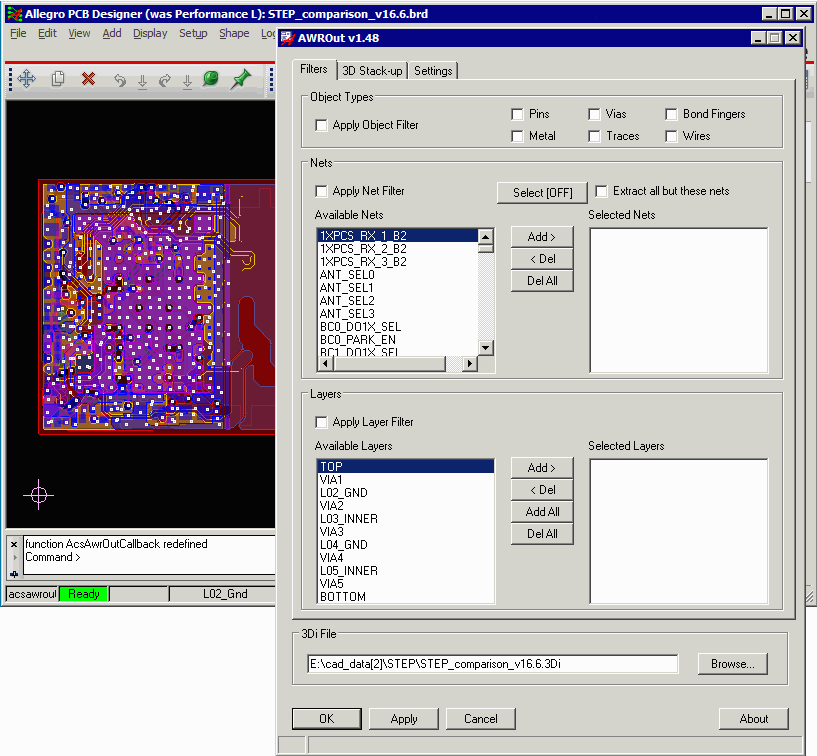
The main dialog needs no user input. We'll go to the Settings dialog and adjust our parameters.
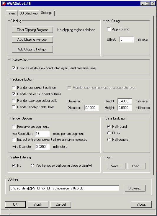
We are not clipping out any region of the board (we could if we wanted to)
We are unionizing all data on conductor layers - this avoids collisions/interference in 3D between shapes/pads, shapes/clines and clines/pads that might cause the mesher to fail.
Since we're not interested in components we don't check: Render Component Outlines
We are interested in our substrate dielectrics so we check: Render dielectric board outlines
We are using 16 segments per circle for our arc fracturing on our conductor layers.
AWROut Settings
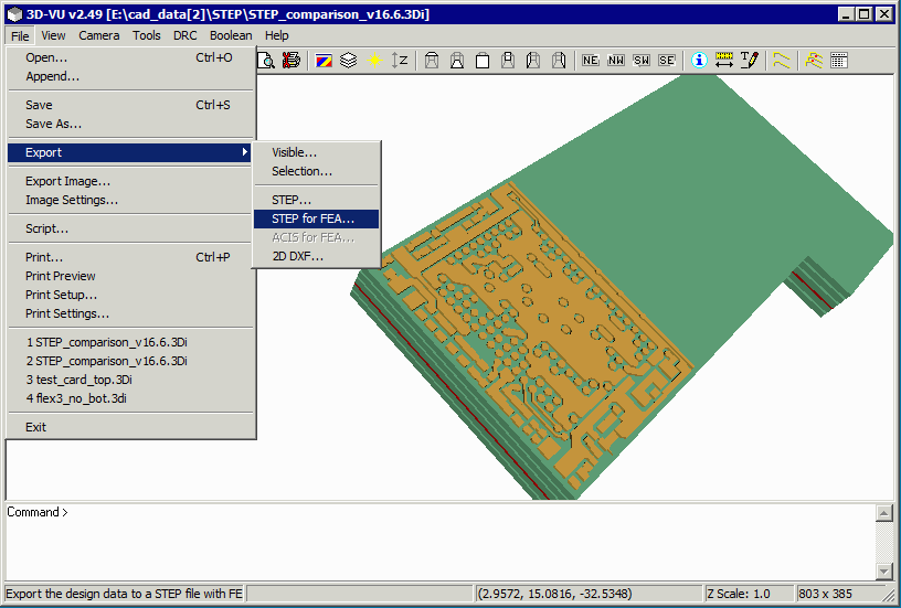
Next, we'll use 3DVu to open the 3Di file and export STEP.
Start by opening the file and selecting File | Export | STEP for FEA
|
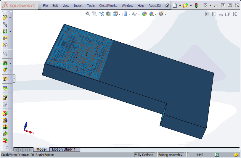
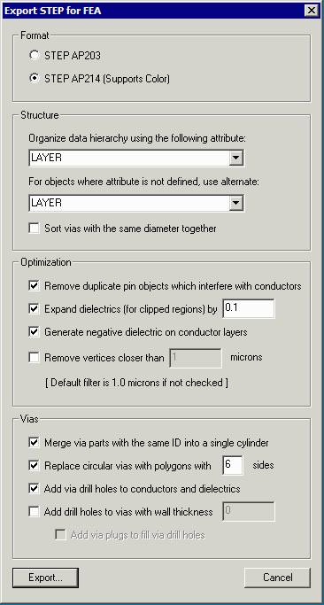
Our STEP Output Settings We'll produce AP214 (standard STEP with color attributes) We'll organize/sort the output by layer. We'll remove any duplicate pin objects (not necessary in this case but a good check) We'll expand our dielectric body by 0.1 mm (insures a safe Boolean for the next step) We'll generate negative dielectric to fill in the air gaps on each conductor layer. We'll merge our via stacked cylinders into a single long cylinder We'll force our vias to have 6 sides in the crossection to reduce mesh count Wherever a via passes through a conductor or dielectric body we'll "drill" a corresponding hole. We're not going to create hollow vias (though we could). |
 |
File Size Differences?
When we look into our directory we see that the two STEP files produced vary greatly in size! The Artwork file is more than 100X larger than the STEP file produced by Allegro.
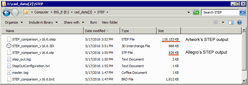
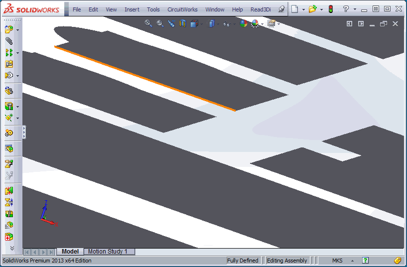
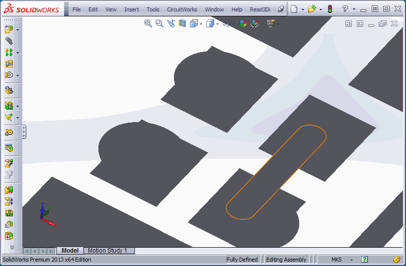
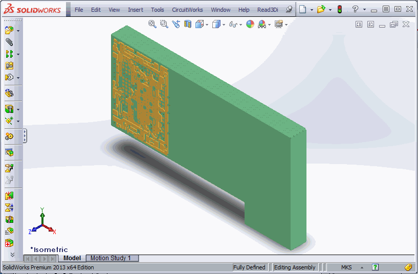
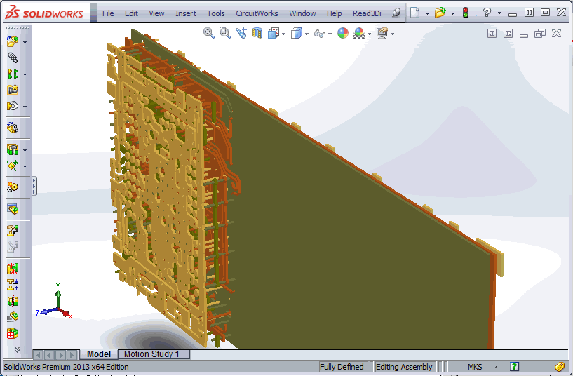
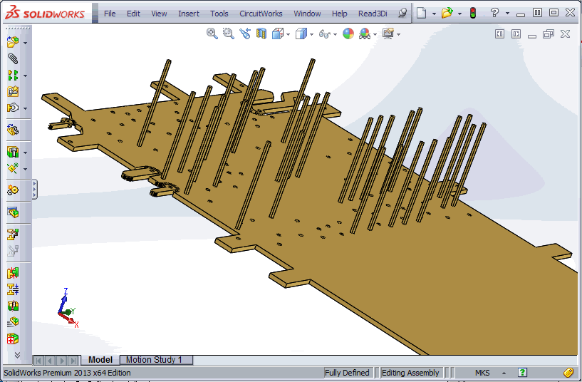
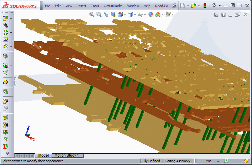
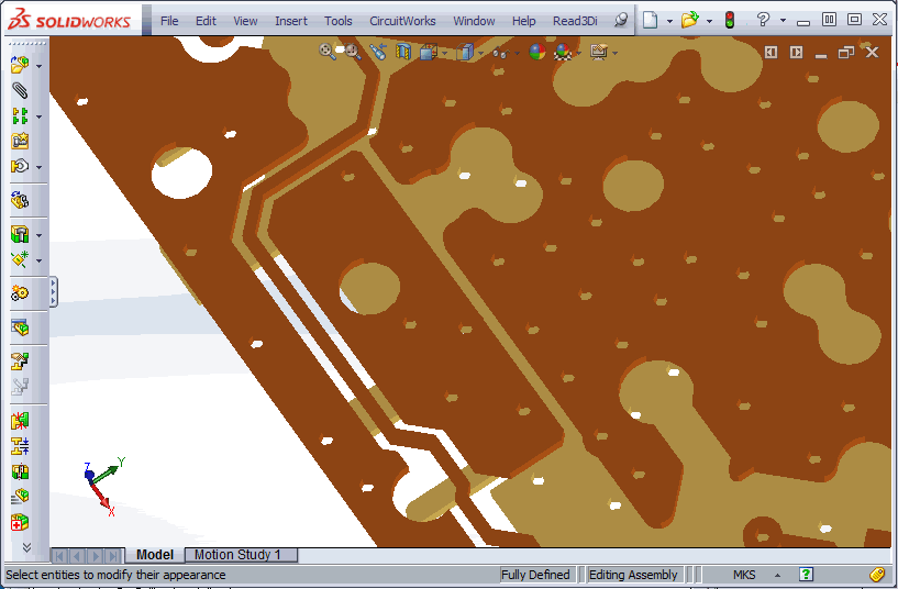
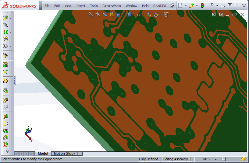
Can this be correct? Let's open both files in SolidWorks and find out.

