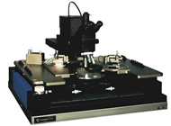
Wafer Map Format - Cascade Microtech PA 200This format is produced (and read) by the Cascade Microtech PA200 prober (and possibly other probers from Cascade). It is saved with the extension .map (though other formats also use the same extension such as those from EG) |

|
The map file is broken into sections delineated by square brackets.
The Header Section
This section includes a description (always set to Wafer Map File) and the version of the Wafer Map File.
[Header]
Description=Wafer Map File
Version=1.3
The Wafer Section
This section describes the wafer and various parameters associated with the array.
[Wafer]
Revision=0.0              always set to 0.0
Diameter=70               diameter in mm
FlatLength=15.9           the length of the flat in mm
FlatAngle=0               0=bottom, 90=right, 180=top, 270=left
EdgeArea=0                the margin (mm)
XIndex=10000              die pitch in um
XOffset=0                 offset from X for first die from the wafer edge (%)
YIndex=10000              die pitch in um
YOffset=0                 offset from Y for first die from the wafer edge (%)
Shape=Wafer               Wafer=Round (Rectangle)
DieInX=7                  For Rectangle the number of die along X
DieInY=7                  For Rectangle the number of die along Y
Origin=UL                 Origin of the coordinate system (UL,UR,LL,LR)
DieMapStyle=Single        Only a single Map
HomeDie=1,1               Coordinates of the home die (absolute scale)
                          Default = 0,0 (The home die defaults to the leftmost
                          and topmost device marked to probe.
RefDieOffset=0,0          The offset of the origin from the home die.
UseClusters=0             don't really know
ClusterSizeX=1            don't really know
ClusterSizeY=1            don't really know
TestFrom=2                for clusters - which die to test first
TestFaulty=0              for clusters
RouterStartColumn=Left    Defines the column of the first die to probe (Left | Right)
RouterStartRow=Top        Defines the row of the first die to probe (Top | Bottom)
RouterType=HorSingleDir   defines the type of path followed by the prober (see illustration)
                          HorBiDir | VerBiDir | HorSingleDir | VerSingleDir | XYOptimized |
                          XOptimized | YOptimized
The Bin Definition Section
The bin section defines the various possible die bins. There are a total of 256 bins (0-255)
The first parameter in the line BIN=VISIBLE (0|1) where 1=Visible
The second parameter is a two character bin code
The third parameter is a color definition (RGB Hex) that can be used by a viewer
The next parameter is a Boolean - (0|1) where 0=FAIL and 1=PASS
The last 4 parameters are for the inkjet heads (1=SET, 0=Not SET)
[Bin]
0=1,a0,00C000,1,0,0,0,0
1=1,a1,0000FF,0,0,0,0,0
2=1,a2,FF0000,0,0,0,0,0
3=1,a3,FFFF00,0,0,0,0,0
4=1,a4,FFFF80,0,0,0,0,0
5=1,a5,808000,0,0,0,0,0
.
.
.
252=1,W0,FF00EA,0,0,0,0,0
253=1,W1,FF00F0,0,0,0,0,0
254=1,W2,FF00F6,0,0,0,0,0
255=1,W3,FF00FF,0,0,0,0,0
The Die Section
This section lists each die by number in the array, its status and the probe result.
The die number is the number of the die when they are enumerated from top to bottom and from left to right.
The available status parameters are:
   X     = invalid or invisible die
   P     = a die to be probed
   I     = a die to be inked but not probed
   V     = a valid die but should not be probed
   0-255 = die was probed and has the designated bin value
[Die]
0=X
1=X
2=X
3=X
4=X
5=X
6=X
7=P
8=P
9=P
10=X
11=X
12=X
13=P
14=P
.
.
.
The Process Section
Contains identification information about the wafer.
[Process]
WaferID=
ProductID=
LotID=
WaferNum=1
