Glossary of Wafer Map Terms
Wafer
The round wafer used to build chips typically has a diameter of 200 mm or 300 mm. A flat or a small notch is cut into the wafer in order to align it in a repeatable orientation during each step of processing. The wafer map must inform the user of the location of the flat or notch.
Flat Location is either labeled as BOTTOM,LEFT,TOP,RIGHT or in degrees: 0,90,180,270. Unfortunately, when using degrees some map formats do not agree about whether 0 degrees is on the top or bottom.

Binning
Binning is the process of assigning a bin code to each device on the wafer. Devices may be optically inspected and/or electrically tested. Some are completely rejected. Those that pass may be assigned grades based on the electrical test.

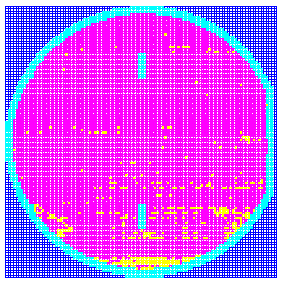
Blue: Null Bin; Cyan: Edge Bin (or Skip); magenta: good/pass; yellow:fail
bin code - the character or number assigned. Some maps use a single ASCII character; others may use a HEX value (i.e. FF) and others may use a single digit or 3 digit bin label.
null bin - since the array is rectangular and the wafer is round, in order to keep track of the proper location null or empty positions are assigned using the null bin code. This is often the dot character; for SINF the null code is two consecutive underscores __. There are certain types of map encoding that do not require a null bincode.
reference bin - a reference die (also known as an alignment die) is one that the machine processing the wafer uses to properly align with the wafer map. It may or may not be a "good" die. Often it is visually distinct (and hence not a "good" die).

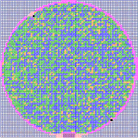
two reference devices (black): upper left and lower right
mirror bin - a mirror die is one that is highly reflective -- the equipment is able to find the mirror die from a full wafer view. Mirror die are often placed adjacent to a reference die.
ugly bin - an ugly die is typically one which may not be complete because it was either damaged during processing or is located in a region where it has been truncated.
edge bin - an edge die is one near the periphery of the wafer and is rejected because processing near the edge is not consistent.
fail bin - any die binned as fail will not be "picked" for further processing.
pass bin - a die which has been tested and found to be in spec - it will be picked.
first die - some maps identify the "first" die - i.e. the one that was probed first - whether it is good or bad.
skip die - for one reason or another, the probe machine has been instructed to skip testing of this die. Some maps may assign SKIP die the same bin code as NULL die.
Map
map overlay - a term used in SEMI E142 for the array of bin codes associated with a substrate/layout. E142 allows multiple maps to be "overlaid" on a single substrate. For example, if more than one test were performed, the results of each test could be recorded in separate maps. However we rarely encounter this and currently don't support it.
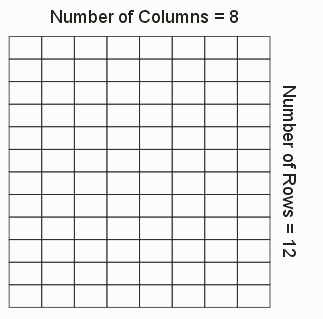
array dimension
- the X and Y dimensions of the map array. This includes the null die positions. Do not confuse the use of dimension here with a physical length -- it is the size of the array (positive integers only)

rows - the number of horizontal rows in the array.
columns - the number of vertical columns in the array
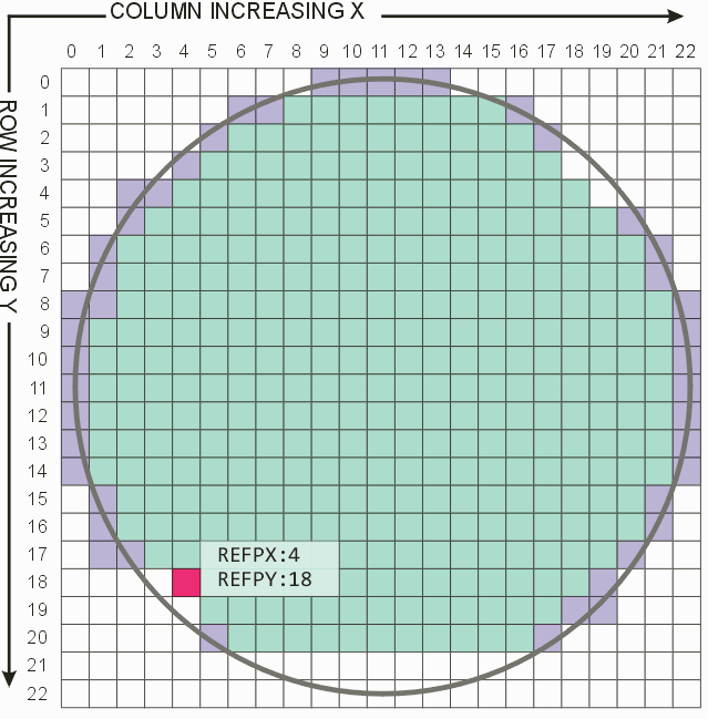
origin location
- one of the 4 possible corners where the array count begins. Labeled either by quadrant (I, II, III, IV) or by name: UpperLeft, LowerLeft, UpperRight, LowerRight

axis direction
- the direction in which the array indexes increase for X and for Y. Typically for an origin in the LowerLeft the Axis would be UpRight. However nothing prevents a different axis direction (which often results in negative index values.

Reference Coordinates
- a map file will often state the location (or locations) of reference devices by the array position i.e. REF1: 129,26. It is necessary to know the origin location and axis direction to actually find the reference die. It is also necessary to know whether the index count starts at 0 or 1. (Most maps start at 0 but a few we have seen start at 1. And at least one starts neither at 0 or 1 but sets 0 to the location of a reference die.)

Die Size and Stepping
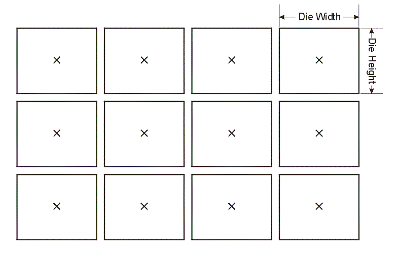
Die Size - the X and Y dimensions of the die that is stepped across the wafer.

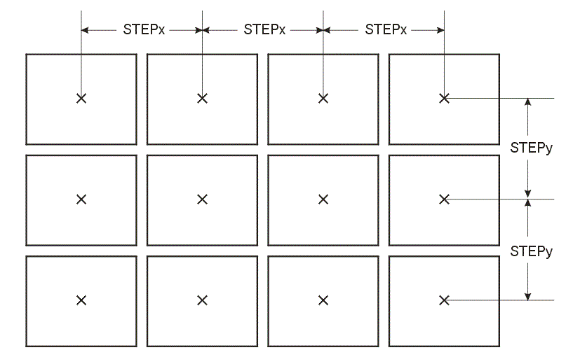
Step Size - the distance from the same point on a die to the point on an adjacent die; often referred to as pitch. This is typically larger than the device size - for most wafer map users this is the number that is of interest.

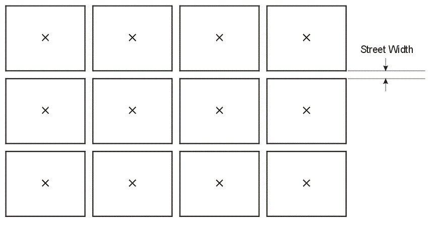
Street Width - the gap between the edges of adjacent dies. It is there to account for the width of the saw used to singulate the die. This information is typically not useful for equipment that uses the die map. Step Size - Die Size = Street Size.

Identification
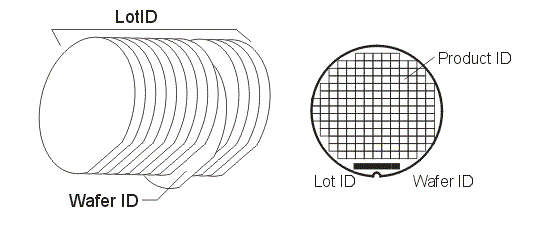
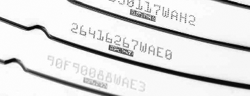
LotID - wafers are normally fabricated in lots - typically up to 25 wafers per lot. The Lot ID is the number or string assigned to the lot by the fab. It is generally etched into the wafer so it can be read by man and machine.


Wafer ID scribed into the margin area of the wafer. You can also see the notch.
Wafer ID - each wafer within a lot is assigned a unique number or string. This is also etched into the wafer.
Device ID - identifies the device that is stepped across the wafer.
Product ID - often used interchangeably with the Device ID.
