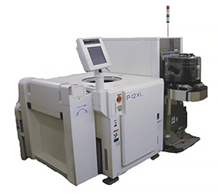

The TEL P12XL outputs a group of files containing the wafer map data.
<wafer_name>.DA

FORM.DA

LOT.DA

<wafer_name>.RMP
This prober supports wafers up to 300 mm in diameter. The binary map format for the P12XL can differ from that of the earlier P8 series of probers in order to support a larger number of devices on the wafer.

| File Name | Data Type | Comments |
|---|---|---|
| FORM.DA | ASCII | Single Character: 1 | 2 defines format option |
| LOT.DA or LOT<n> | ASCII | Contains: LotID, WaferID, Wafer Size, Flat Angle, Device Size |
| <wafer_name>.DA | ASCII | Contains: Start Time, End Time, Wafer Number, Cassette Number, Slot Number. |
| <wafer_name>.RMP | BINARY | Contains:Map Data |
If the supporting ASCII files are missing (i.e. only the .RMP file is supplied, then one can see the array along with the pass/fail and bin codes but one will not get the rest of the map information such as device stepping, LotID, DeviceID, Wafer Diameter or Wafer Flat/Notch position.