Like most wafer map formats, the E5-1296 map format starts with a header section followed by the bin map section.
WAFER MAP = {
the curly bracket indicates that a list of parameters is enclosed.
WAFER_ID =
Wafer Identifier. A string (enclosed in double quotes) up to 16 characters long. Usually matches the information scribed onto the wafer. Spaces are allowed inside of the double quotes.
MAP_TYPE =
A string describing the map type. Most typical would be ASCII.
NULL_BIN =
The character used to present locations for which there is no data. Use the "." for maximum compatibility.
ROWS =
The number of rows in the array
COLUMNS =
The number of columns in the array
FLAT_NOTCH =
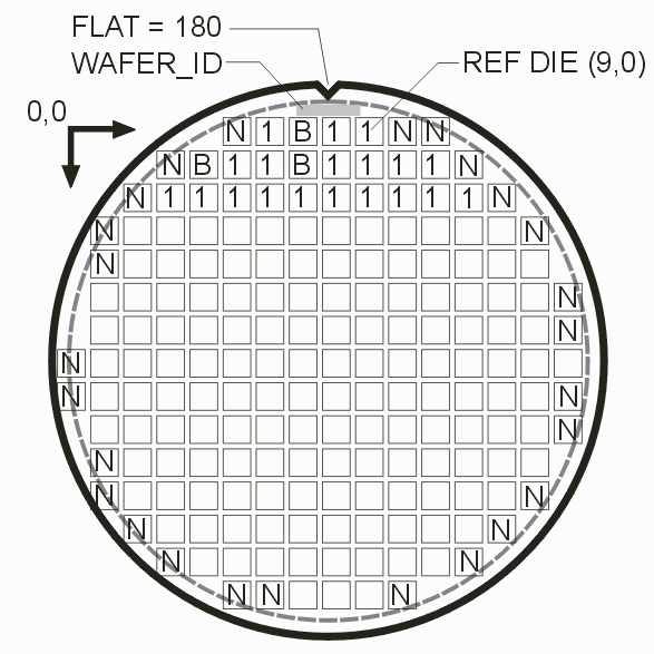
The position of the flat or notch on the wafer for the data presented in the map section. 0 | 90 | 180 | 270
SUPPLIER_NAME =
A string identifying the supplier of the wafer. Enclose in double quotes. Max 16 characters.
SUPPLIER =
recently saw a file that used SUPPLIER as the keyword instead of SUPPLIER_NAME.
LOT_ID =
An string identifier generated by the wafer supplier to group together a number of wafers - either by process, test or other grouping.
WAFER_SIZE =
recently ran across a file that had keyword WAFER_SIZE in it.
X_SIZE =
The pitch between devices along the X axis. Always in units of MM. (5 digits: two to the left of the implied decimal point and two to the right of the implied decimal point. So a number such as 620 represents 00.620 mm)
Y_SIZE =
The pitch between devices along the Y axis. Always in units of MM. (5 digits)
REF_DIES =
The number of ref dies (only 1 integer may be used so max = 9)
REF_DIE =
The X and Y array positions of the reference die(s).
BINS =
Recently ran across a file that had this keyword in it. It appears to indicate the number of bin codes defined. This number does not appear to include the NULL Bin definition.
BIN =
Each BIN line contains four fields which are space separated. When devices are tested (or even skipped) they are assigned a bin code.
Field 1 - a single character - known as the bin code - such as 1,B,N indicating the test result (enclose in quotes)
Field 2 - an integer indicating the number of die in that bin
Field 3 - a character string (in quotes) such as "Pass" "Fail" "Not_Used"
Field 4 - a character string (in quotes) for further description. This could be used to differentiate different devices that passed or failed.
DIES =
recently ran across this keyword that seems to define either the total number of devices tested or the total number of passed devices.
MAP = {
The keyword indicating that the map data follows.
Each map consists of a row of bin codes starting at the top left of the wafer. There are no spaces between the bin codes. While other types of maps may be supported, we have not seen any such E5-1296 files that use a map other than single character ASCII.
...N1B11NN...

..B11B1111N..

.1111111111N.

N1111111111B.

1111B1111111N

111111111111B
}}
two right curly brackets are needed at the end of the file to close the WAFER_MAP= { and the MAP= { sections.
Naming Convention
E5-1296 map files are generated based on the wafer's scribed identification. The WAFER_ID is then followed by the suffix .txt indicating that it is a text file.
Example
Wafer ID = A12345-01A5 Filename: A12345-01A5.txt
Flat Orientation

Reference Die
The reference die is the top right die with probe marks (i.e. the top right tested die)

Ugly Die
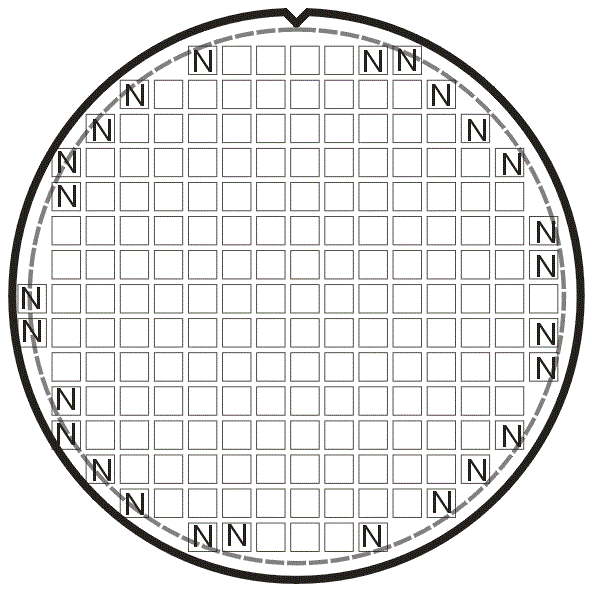
Die that fall within the 3 mm edge of the wafer are classed as "Not_Used" (N) -- often known as Ugly Die.
