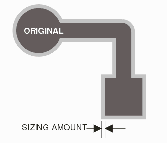

QckBool enables sizing up (expansion) and down (contraction) while simultaneously unionizing the data. Sizing is most often used to compensate for over or under etching during the manufacturing process.

Sizing is always measured from the edge of the shape. If you size a 10 um line up by 1 um, then the final width of the line is 12 um.

Sizing is controlled from the Boolean Operation Settings dialog box. The default value (0) turns off the sizing operation.

|
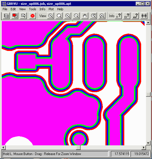
Below is an example of a PCB top layer (pads, traces and ground plane) that has been sized up:  The magenta layer is the original size (the oblong pads are 0.024 inches wide.) The green is sized up 0.002 inches, the blue is sized up 0.004 inches and the red is sized up 0.006 inches. The sizing value should normally be significantly smaller than the feature size of the pads and traces; otherwise there is a possibility, particularily where the shape has sharp turns or indentations, of distortion in the final results. There is also the chance that if the sizing value is larger than the gaps between conductors that independent nets become shorted together. |
| Home | Download | Price | Rev History | PDF DataSheet |