Distorted Geometry
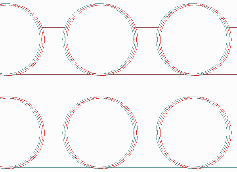
Let's zoom in at our geometry at 7 different locations on the wafer and examine what the distortion module has done. We are going to overlay the CAD source data over the corrected data using Artwork's Qckvu3 GDSII viewer and our SFF Merge plug-in that enables the overlay of two separate files.
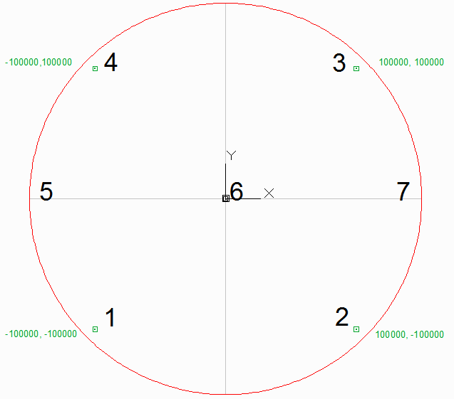
Location 1: As this is our reference corner we expect little or no difference between the original and corrected data. For reference, the tiny square pads connecting to the die openings are 9 um across and the line widths are 1 um. (original data is in blue and corrected data is in red.
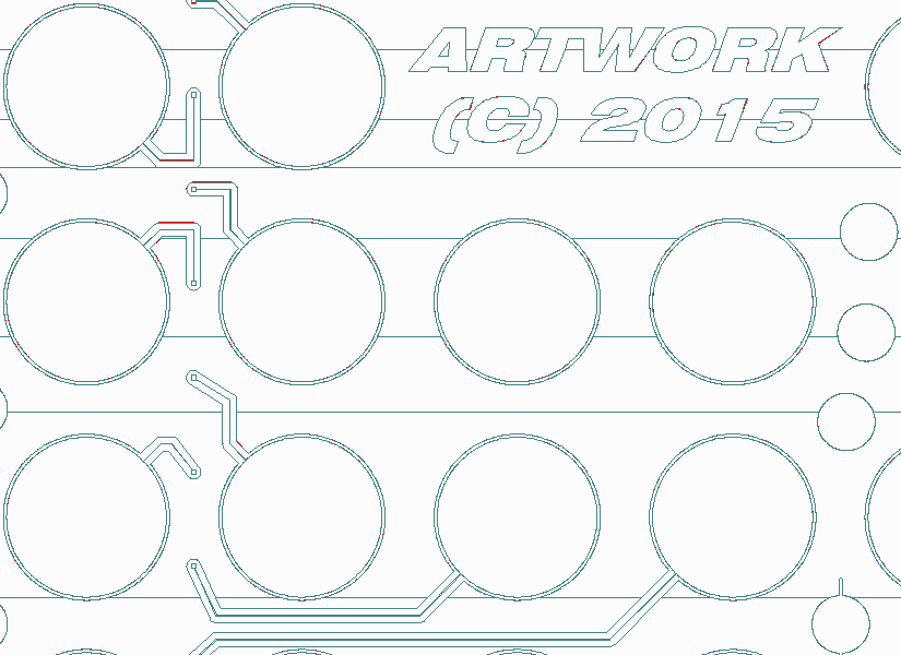
And as we see, there is no measurable difference here between the uncorrected and corrected layout.
Location 2: We expect that the corrected data will be "out" along X and "down" along Y.
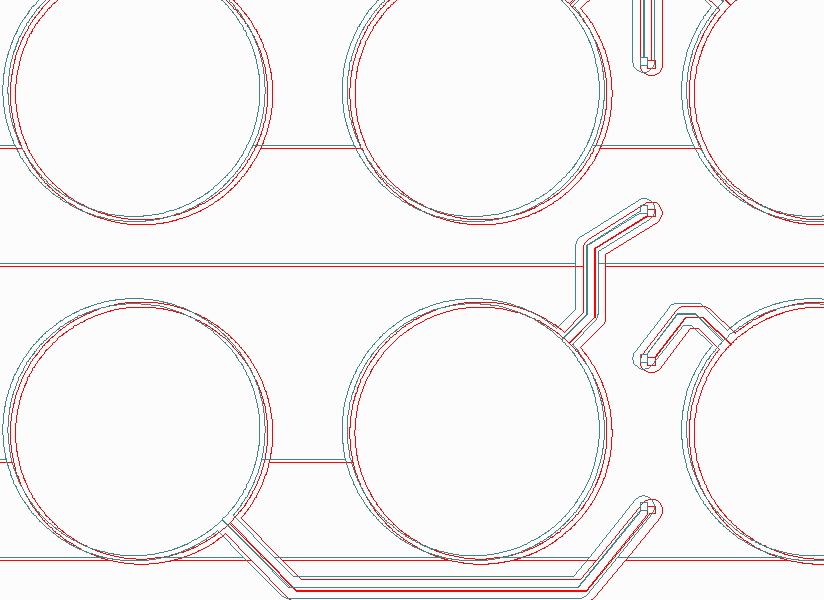
As we input a delta of 9,-4 in this location we expect to get that amount. And if we carefully measure the difference of the 9 um pad center we see that it is:
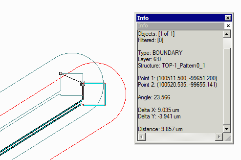
Location 3: We expect that the corrected data will be "out" along X and "up" along Y.
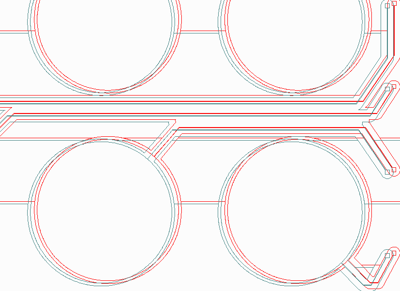
Location 4: We expect that the corrected data will be "out" along X and "up" along Y.
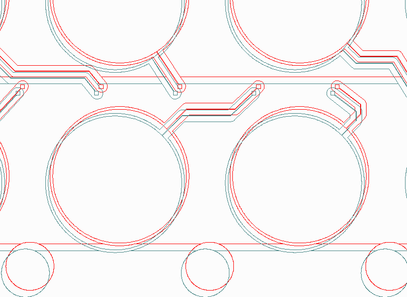
Location 5: Notice that location 5 is "outside" the domain defined by our correction data. Nevertheless, it is still corrected using some extrapolation.
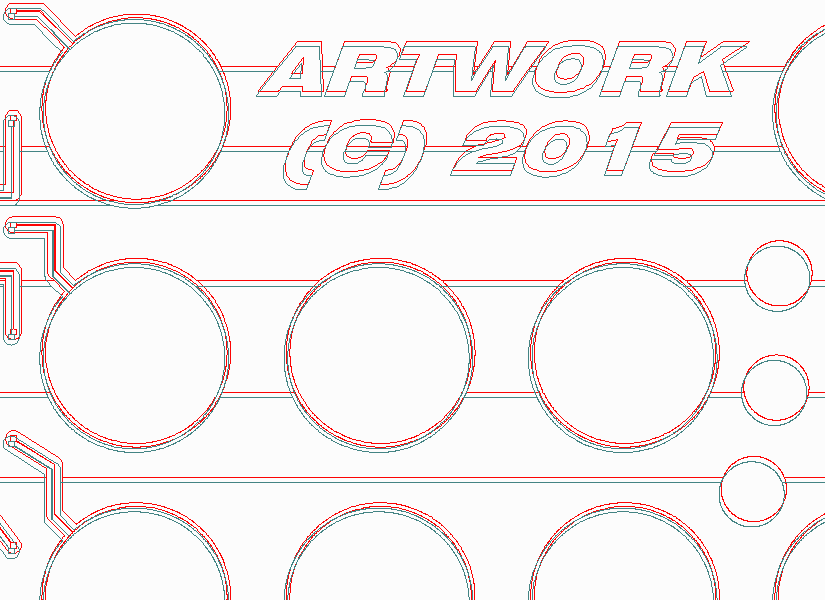
Location 6: We are in the center of the wafer and the correction should be an average of the compensation found in the 4 corners since they are equidistant.
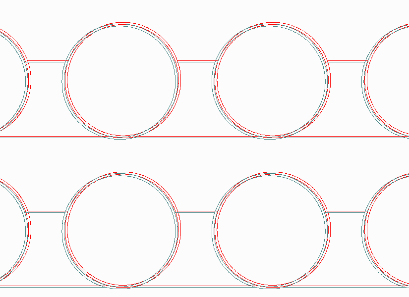
Location 7: Again, we are outside the domain but correction will be extrapolated and applied.
