AutoCAD for PCB Artwork

Steve DiBartolomeo
Applications Manager
Artwork Conversion Software, Inc.
© 1995 Artwork Conversion Software, Inc.


Introduction

This document explains how to use AutoCAD to draw printed circuit board artwork. The methods described here are not the only ones that work, but have been successfully applied to both simple and complex boards. The drawings are converted to Gerber using Artwork Conversion Software's ASM 500. Two types of boards will be discussed:

  • A two-sided PCB

  • A multi-layer board with power and ground planes


The Two-Sided Board

The two sided board requires several photo tooling films. AutoCAD layers that should be defined are:

  • Padmaster (PADM): pads for thru-hole component and vias

  • Solder side traces (SOLD): circuit traces, areas and smd pads on the solder side of the PCB

  • Comp side traces (COMP): circuit trace, areas and smd pads s on the component side of the PCB

  • Solder Mask: solder mask for top (and possibly bottom) side of board.

  • Silkscreen (SILK): component outlines, part numbers and the board identification

  • Targets (TARGET): alignment targets and mask ID for all layers
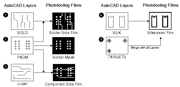

illustration of AutoCAD layers mapped to Gerber output.


Why Organize This Way?

This organization was developed so that board fabrication information can be easily extracted from the drawing data and the Gerber files. For example, the padmaster is normally used to also create the drills needed for vias between top and bottom sides of the PCB.

Solder Masks

Defines openings in a protective plastic coating that covers the top and bottom side of the PCB. Thru-hole pads, SMT Pads and test points are exposed and traces are covered.

If the drawing is properly organized, the solder masks can be derived from the padmaster layer and the flashes on the top/bottom side of the PCB.

The board fabrication shop uses a CAM tool to extract these pads from the Gerber and then sizes up the pads slightly to define the solder mask opening. the pad dimensions slightly and replots the data to get the


Drill Data

Vias are formed by drilling a hole through the PCB and then plating the inside of the hole. A drill file is similar to a Gerber file; it generally consists of a tool selection command followed by a list of X,Y coordinates where holes are drilled. Normally these locations are extracted from the padmaster layer.

  pcbap_2.gif


Bare Board Test Points

Before populating a bare PCB it is run through an electrical test to insure that there are no short circuits or broken connections. To do this testing one normally needs the location of all the IO points to test and what nets are connected. While this is not easily put into AutoCAD, the actual locations of the pads can be extracted if the designer has used flashes for all component pads and for any via pads.


Setting Up Your Drawing

Use a grid snap if possible. An exception would be round test boards and some flex boards which do not conform to a rectangular grid. Most PCB fabrication equipment runs on grid based rules. Ask your board fabricator what grid size is supported. Depending on the density of the design, the grid snap may vary from 0.010 inch to 0.001 inch. Once advantage of using AutoCAD is that you can set any grid size you want. If you are working with metric parts you can draw directly in millimeters or set up a grid in inches equal to the proper metric grid.

  pcbap_4.gif

Use grid snap whenever possible; Your drawings will be easier to fabricate.


Use Blocks for Flashes

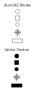
The typical PCB has hundreds of pads for component pins and vias. While you could draw each pad on AutoCAD as a donut or circle, there is a more effective way to create this that carries some useful intelligence downstream. The trick is to create a Gerber flash for component and via pads.

The closest AutoCAD entity to a flash is a block. One drawing approach will be to define a block for unique flash size/shape.

First determine the size and shape of your pads. In our two-sided example we will have .050 round pas for vias, an .060 square pad for pin 1 on components, a .060 round pad for component pins, a .250 x 0.050 rectangular pad for the edge connector, and an alignment target. Although a target is not really a pad, it should always be flashed so that reference coordinates can be extracted for drill data.

Next assign a unique and descriptive block name for each pad. Each block will later be assigned to a Gerber D-code. The block name should be short but descriptive of the flash.

  pcbap_3a.gif

Pad Dimensions Shape Block Name
.060 circle RND60
.060 square SQ60
.050 circle RND50
.150 target TARGET
.250 x 0.050 rectangle RE250X50


How to Create Flash Blocks

Set layer 0 to the current layer. What you draw is only symbolic of what will show up on the film.

For this example draw a .060 diameter circle, a .050 diameter circle, a .060 square, and a rectangle .250 long by 0.050 wide on a layer PADM.

pcbap_5b.gif

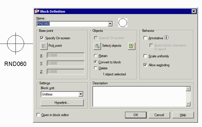
Define each figure as a block. Use the center of the figure as the reference point of the block. Give each block a short name.

pcbap_5c.gif

When placing pads you will use these blocks on the desired layer. When running the conversion from DXF to Gerber, you will assign each of these blocks to a unique D-code. The descriptive name will help in building the aperture list.


Inserting Flashes

Set the current layer to PADM. Using the block insert command, insert the block RND 060 for component pins. You may wish to create a macro or an AutoLisp routine to speed things up. Repeat this for each pad type you use in the design.

pcbap_6a.gif Inserting blocks for flashes


Building Libraries

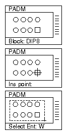
It often makes sense to build a block containing all of the required pads for a part and the outline of a part. To create a library element, first set the current layer to padm. Insert the blocks required for each pad. Change the current layer to SILK and draw the part outline.

Then define a new block using a name that represents the part. This block will contain blocks such as RND60 and SQ60 and will also contain the part outline on the layer SILK.


pcbap_6a.gif

pcbap_7a.gif
Building libraries using flash blocks. Do not set the block DIP8 to a flash

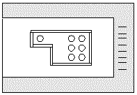
Do not insert flashes or blocks containing flashes or rotation   pcbap_8.gif


pcbap_9.gif


By building your own library of blocks, time can be saved. Flash blocks should be inserted on layer PADM. Part outlines should be drawn on the silkscreen layer.

Drawing Circuit Traces

Circuit traces are drawn using AutoCAD's POLYLINE entity. The polyline can be assigned a width and can have many vertices. Don't use AutoCAD's trace entity; although it may sound like a good entity to use, it actually consists of separate polygons and is not efficiently converted.

pcbap_11.gif


Polylines are translated to a Gerber stroke of the same width. To draw circuit traces on the solder side of the board, set the current layer to SOLD. Using polylines of the width chosen for your traces, connect the pads.

Polylines can be adjusted using the PEDIT command to move vertices or change the width. Polyline arc sections may also be used, especially of flex circuit boards. Each Gerber stroke will have a 1/2W round extension at the ends of the stroke because it is created by a pen with diameter W.

pcbap_10.gif


Solids

For certain designs you may desire that some polylines are treated as boundaries (i.e.,the square end is preserved) and others are treated as circuit traces. The simplest approach is to use AutoCAD's "SOLID" entity for all rectangular pads. Use polylines to interconnect the SOLID's. The SOLIDS will be filled so that the edges remain square. The polylines will be plotted using a single aperture.

  Ground Planes

How best to draw the ground plane area depends both on the complexity of the ground plane you wish to create, and on the capabilities of your translator and phototherapy. It may be difficult to visualize your ground plane area because AutoCAD lacks the ability to display an irregular filled area. Several strategies are outlined below.

Hatching

Very simple ground planes can be hatched using AutoCAD's hatch command. A simple translator such as ASM 501, which does not fill closed areas can still be used for ground planes. Hatching quickly becomes ineffective because:

  • AutoCAD stores th hatch information as a block of lines. This increases the fill size and slows down redraw and regeneration.
  • It is not easy to compensate the end of the hatch lines resulting in leaks past it's boundary.
hatch1.gif AutoCAD's Hatch can be used to fill simple ground planes

Closed Area Fill

Translators such as ASM 502 and ASM 500/386 will fill closed zero-width polylines during the conversion. With these translators, you can create your ground plane using a zero width closed polyline. The post processor will stroke the interior, automatically compensating for aperture diameter.

Translators such as ASM 502 and ASM 500 fill closed areas. These translators also compensate for aperture diameter. hatch2.gif

It's very easy to draw, and drawing file size remains small. However, AutoCAD will not display the fill on-screen. If you have areas inside the ground plane that need to be cleared, the auto fill will not take these into consideration.

hatch3.gif These translators do not take in account areas the designer wishes to remain clear.

Fill-on-the-Fly Photoplotters

Even better, use a photoplotter that can fill areas during rasterization. Both the drawing file and the Gerber file stays very small. Photoplotters that can do this include model 9825 from Gerber Scientific, the FIRE 9000 family from Cymbolic Sciences, and the photoplotter from Mivatec.


Negative Plot

Some layers are almost all ground plane. In this case it is best to draw only the clearances. This data can be reversed on the photoplotter and merged with a trace or pad layer if necessary.

hatch4.gif

Sometimes it is easier to draw just the clear areas.
  pcap_14a.gif

Film can be easily reversed on the plotter

The Silkscreen Layer

The silkscreen layer usually contains component outlines, text, and perhaps a company logo. ASM 500 reproduces text by using the same SHX font files as AutoCAD. The font strokes are converted to Gerber draw commands after the appropriate scaling, rotation, and mirroring. You will need a copy of the SHX file available to the translator when running the conversation.

Logos can be drawn by outlining the border and then hatching the inside.

Set the current layer to SILK. Construct the outlines for IC's, resistors, capacitors, etc. Make a note as to how thick you want these lines to be.

A thickness of 0.008 to 0.015 inch is recommended. Check with the board fabricator for the optimum width.

You may, if you wish, define each outline as a block or incorporate it into a library component. This will enable you to place a large number of outlines quickly. When the postprocessor encounters an inserted block, and does not find the name in the aperture table, the post-processor explodes the block and then processes the entities found outside of the block.

The entity data must be located on the layer under consideration. You should not draw your component outlines on layer 0 and then expect to find them in layer SILK, even if you insert the block in layer SILK.

pcp_15a.gif Silkscreen text should not be so thin that it does not produce a clean screen, nor should it be so thick that it blocks up. As a rule, make the text thickness about 1/7 the height.

pcp_15b.gif For the font panel work, custom fonts can be obtained that use multiple strokes to emulate well known typefaces such as Helvetica.

pcp_15c.gif Logo's can be drawn using lines and arcs and the filed by hatching

Pad Clearance

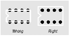
It is considered bad practice to run silkscreen ink over pads. While board fabricators now have CAM programs that can remove lines that cross over pads, it is better if the designer avoids this practice.

pcap_16a.gif
Block Attributes

AutoCAD's Block attribute is a useful tool for those building part libraries. The attribute is a piece of text that can be attached to the block. The beauty of the attribute is that the text string can be set up to be a variable - at the time you insert the block, the designer is prompted to enter the desired string of text.

This is ideal for adding reference designators such as U1, R11, C5, as well as component values. Unfortunately, on dense boards you can not always locate the part number or reference designator in the same position relative to the block insertion point.


Multilayer Boards

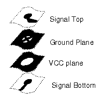
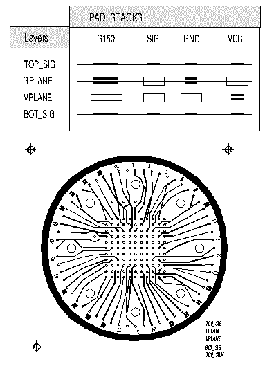
Multilayer Boards include multiple signal layers, ground layers, and power plane layers. In this example, we will use a board that has a top and a bottom signal layer, one ground layer, and one VCC layer.

pcbap_17.gif
Ground and power plane layers do not normally contain traces. They contain either clearances or connections to the metal in the plane. The connections to the plane are made via a "thermal", for the purpose of keeping heat away from the flowing copper during soldering.

Pad Stacks

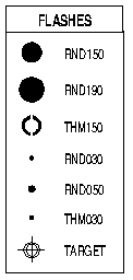
Unless you have a very complex board with inner layer vias, you can set up a family of road stacks to ease your design. First determine the different flashes you will require. In this example we need:

Description Block Name Purpose
Round.150 RND150 Screw Holes
Round.190 RND190 Clearance of screw holes
Thermal.150 THM150 Thermal for screw holes
Round.030 RND030 Signal pad
Thermal.030 THM030 Thermal for VCC or GND
Round.050 RND050 Clearance for VCC or GND
Target.150 TAR150 Targets for alignment

Then build a block stack consisting of the correct flash blocks on each layer. See the table below. Now insert the correct stack as needed. Once all the stacks are inserted you can interconnect them with polylines.   pcap_18a.gif

pcbap_19.gif


Artwork Home ASM500 Family Home Pricing