Negative (In-fill) Dielectric
When creating a 3D PCB model which you plan to use for thermal/mechanical or even EM simulation, you'll likely encounter a problem that originates with the layer-based model used in 2D. EDA 2D design tools basically concern themselves solely with the conductor patterns on each layer. The dielectric between each conductor layer is taken for granted - about all they record is the nominal thickness.
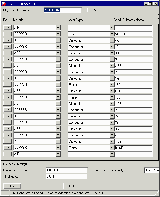
If you extrude each conductor layer and dielectric layer individually then internal to your stackup you will have air gaps.
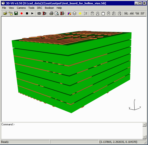
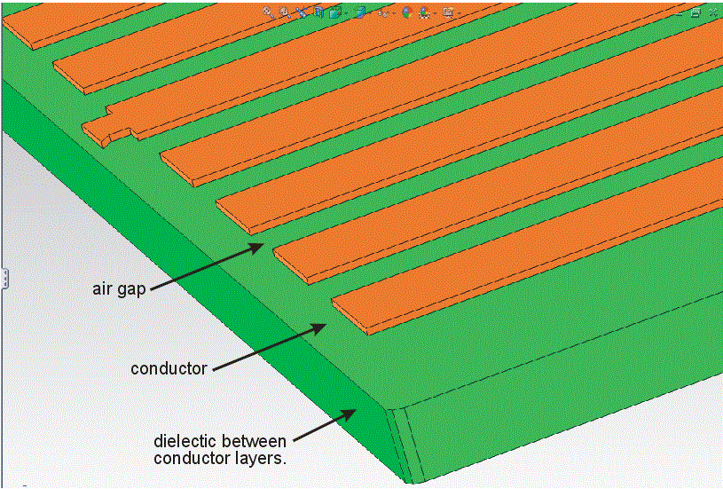
For some applications these air gaps make little or no difference. But if you are using an FEA simulator and meshing the dielectrics then these air gaps will cause a lot of problems.
What's the Solution?
Well the simulation engineer could attempt to "draw" in bodies to fill in the empty regions. But this is a manual and time consuming effort and prone to errors. The bodies must perfectly mate with both the conductors and the dielectric above and below.
Below you can see the top layer as originally extruded.
Artwork's FEA version of 3Di2STEP is able to generate these "fill in" or "negative" dielectrics by using a Boolean function - using the dielectric boundary as the outer limit and subtracting the metal bodies gives us the required bodies to fill in the air gaps.
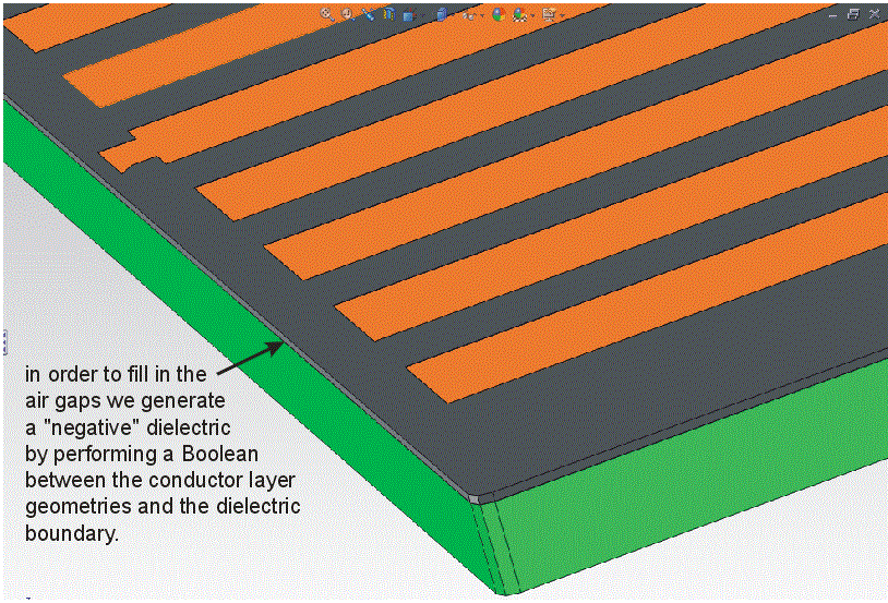
This step is repeated for every conductor layer (including the top and bottom conductors) so that the final collection of dielectric and conductors has no inner gaps.
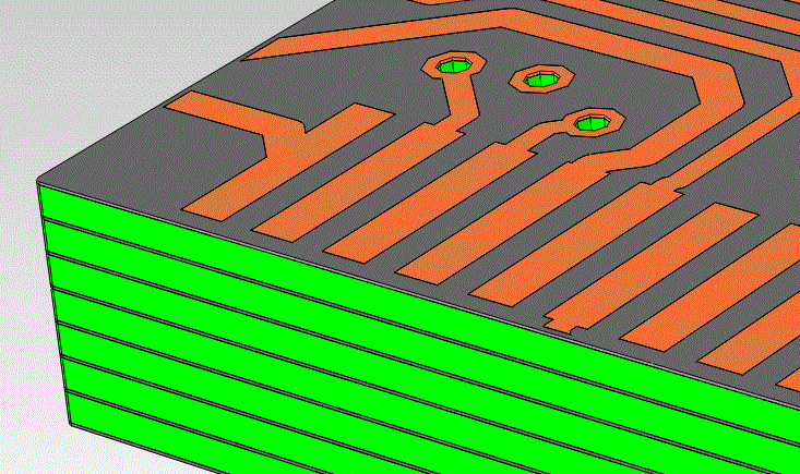
It is an exclusive feature of our FEA software and one that saves a lot of time and effort for the simulation engineer in the preparation of his geometry data.
