This version of 3Di2STEP includes a number of geometric processing steps that increase the usefulness of the 3D data for FEA simulators such as those from Altair, Ansys, SOLIDWORKS, Abaqus FEA by Dassault Systems, COMSOL and others -- particularly for simulation of multi-layer PCBs and vias.
Our FEA users have offered many suggestions to make their lives easier and we've attempted to implement special data processing in order to meet their needs.
Reduce/Control Vertex Count - The FEA mesher must break the surface of each solid body into faces. If the input data has too many vertices then the number of faces goes up and the simulation slows down. So when we convert circular data (i.e round pads or vias) into 3D, we want to provide the user some control over the number of edges/vertices used to approximate each arc.
Perfectly Matching Faces - our STEP data is a collection of solid bodies. Often these bodies share one or more faces and it is critical for the 3D simulator that these butting faces match up perfectly - no tiny gaps or noise in the coordinates of the matching faces.
No Solid Body Collisions - 2D ECAD data often consists of many overlapping structures such as traces and pads. If extruded independently, the resulting 3D file will include many "internal" collisions or interferences. Most FEA meshers do not process such interferences correctly - some may crash and others may produce incorrect meshes.
Useful model for Vias - in the 2D EDA world a via connecting connector layers is simply referenced by mentioning a drill diameter and the layers it passes through. There is no actual geometry constructed in 2D. When we convert this into 3D, however, we have to build a meshable body and we also have to remove material from any other body that the via cylinder passes through to avoid interference. We also have to maintain perfectly matches surfaces at the via/conductor interface (as well as the via/dielectric interface.)
In-Fill Dielectric - 3D CAD models assume layers of conductors with dielectric sandwiched in between but they don't actually create any dielectric solid bodies. These bodies are easy to generate but more difficult is to generated solid bodies for the dielectric that "squeezes" between the conductors on any give layer during the lamination process. For proper simulation you can't leave air gaps between the conductors. [Details]
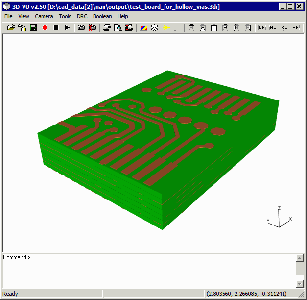
Open a 3Di file using 3DVU.

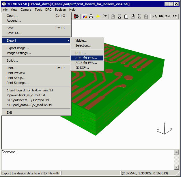
Click on File | Export | STEP for FEA... to launch the STEP for FEA export dialog.

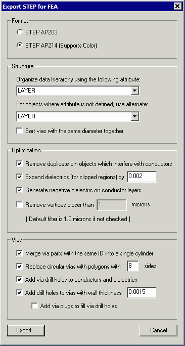
The Export STEP for FEA dialog will appear.

Dialog Options
Format - choose between AP 203 and AP 214. AP 214 support color attributes. You would only need AP203 for very old 3D tools that don't support AP214.
Structure
Organize Data Hierarchy
This drop down enables the user to output the STEP data with different hierarchical organizations. The two common sorts are LAYER and NET. ANSYS EM users have found sorting conductors by NET useful while other mechanical and thermal users generally sort by LAYER.
Attributes with No Object Type
If one selects by NET for the primary sort, this leaves out objects such as dielectrics which have no net assignment. Rather than lump them all into a single "part" it is more common to use the LAYER attribute as a secondary sort.
Sort Vias with Same Diameter
This sort was added for Ansys Maxwell users - it makes it easier to select the vias once in Maxwell and assign attributes to them which are based on their diameter.
Optimization
There are several optimizations that can be performed during the export conversion.
Remove Duplicate pin objects ...
This is needed for the output generated by Artwork's NETEX-G program when converting ODB to 3Di. NETEX-G gets the pin conductor data separate from the layer based conductor information and there is generally a duplication of metal bodies where the components have their pin footprints.
Expand Dielectrics (for clipped regions) by ...
This option is needed when the user clips out a region (using Netex-G or AWROut) and also wants to generate a "negative" dielectric. In order to generate the negative dielectric, a 2D Boolean is done between each conductor layer and the dielectric boundary. If you don't expand the dielectric boundary slightly there is a risk that this Boolean can encounter a sliver at the periphery and fail. By expanding the dielectric very slightly the possibility of such as sliver is eliminated.
Generate Negative Dielectric on conductor layers
This option is needed when doing a FEA simulation; it eliminates the "air" gaps one would find in a simple STEP model that assumed that conductor layers and dielectric layers were fully independent. [Details]
Remove Vertices Closer Than
When the source data contained very closely spaced vertices some 3D tools have a problem processing the STEP data. If you check this box and enter a value the program will search for closely spaced vertices and delete one of them. Note that this might also "distort" the data in some way so we don't recommend setting it on unless you run into problems when it is not turned on.
Vias
These via model options are only available for the FEA version of 3Di2STEP. They produce a model that can be meshed and simulated. [Details]
Merge Via Parts with the Same ID
Since the input is a collection of 2D layers, a direct conversion of vias to STEP results in a stack of cylindrical shaped bodies. This produces a lot of extra work for the mesher. The FEA version of 3Di2STEP is able to merge these stacks into a single cylinder.
Replace Circular Vias with polygons of sides ...
The 3Di database records each via as a circle, center point, diameter and number of sides to render. This allows the user to overwrite the render value and replace it with a different value - typically in the range of 4-8 sides per via. Users have reported very little loss of accuracy when reducing the sides use to approximate a round via but much faster meshing and simulation.
Add Via Drill Holes to Conductors and Dielectrics
If you use the option Merge Via Parts with Same ID to produce a single through via from a stack, you should also check this option to generate the "matching" holes in all conductor and dielectric bodies that the via passes through. This eliminates collisions/interference that can cause a mesher to fail.
Add Drill Holes to Vias with diam ...
Some simulations treat the vias as solid cylinders - others want to treat them as hollow cylinders. To do so, use this option and specify a wall thickness.