DieGen - Die Generator
Package designers must often start work long before the die design is complete. (In fact, this is the proper time -- not after the die is complete and changes cannot be made to accomodate packaging requirements.) However it can be tedious and time consuming to create a "mock-up" of the die - especially larger die with 500 or more staggered die pads.
DieGen lays out a complete die in seconds based on your input parameters - number of die, die pad opening, pitch, and outline size. Additionally, DieGen can distribute around the chip as many power and ground nets as your device will use so that you can simulate your downbonds quickly and easily.
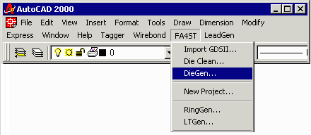
Start DieGen by pulling down from your FA4ST menu and selecting DieGen.
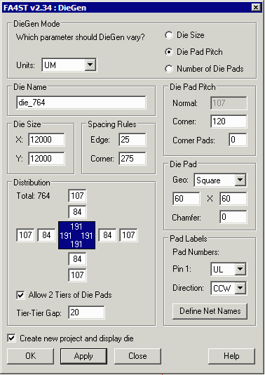
The designer enters his parameters for the die into the dialog box.
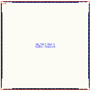
In this example he wants to build a die called "die_764" that has 764 die pads (staggered in two rows).
Die pads openings are 60 x 60 um with a pitch of 120 um and placed 275 um from the corner.
Defining Power and Ground Pads
When designing a package, the power and ground die pads are normally downbonded to rings - these are treated differently than IO pads which go to bond fingers. On a large die approximate 20-25 percent of the die pads are allocated to power and ground nets. Many large die have several different power nets to keep current spikes of off sensitive sections.
DieGen enables you to easily define as many power and ground nets as needed and to define the "percent" of the total die pads allocated to each net. It then distributes these pads evenly as possible around the die.
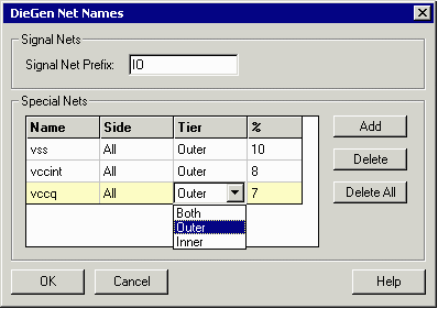
Click on the Define Net Names button.
Then assign a prefix for the IO nets such as IO. Use the Add button to create additional definitions for the power and ground nets. In most cases the power and ground nets willbe distributed on the outer die pad tier.
In this example you can see that we want 10% of the die pads to be our vss, 8% for vccint and 7% for vccq. Obviously given the percentages and the number of die pads these cannot be implemented exactly.
Below you can see how Diegen distributed the die pads for vss, vccint and vccq. The rings and fingers were generated by FA4ST and it was simple to assign each net to a ring.
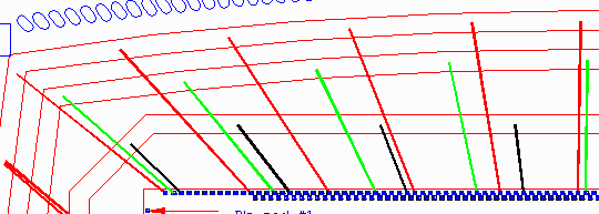
AIF Output
In addition to laying out the die pads on the AutoCAD screen, DieGen creates the AIF file for the chip. This can be imported directly into Encore BGA and Cadence APD
