Introduction to the Program
WMAPLayout is a plug-in that runs inside of Artwork's Qckvu3, GDSII Viewer. The viewer provides the display and measurement functions needed.
Starting the Program
Start up Qckvu3 and then using the Plugins pulldown select: WMAPConvert.

You will see the following dialog that has 3 tabs. The first tab is for creating a layout from the wafer map ascii file. The second tab is for creating a layout from the shot map parameters. The final tab is to overlay the two layouts so that the user can measure the "offset" and then use that to create his template for the RDL mask set.
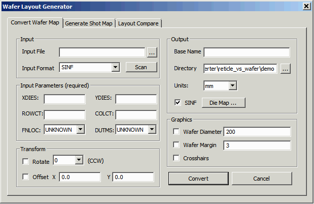
Converting a Wafer Map into a Layout
We'll start by converting a wafer map into a GDSII layout. First we select the wafer map file, wafer_map.txt, to load and scan. A small dialog will pop up that shows what die ID's were found and how many of each were found.
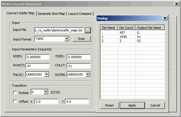
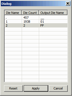
If we want to create a valid SINF file output from this non-standard wafer map input, we need to change some of the die ID's to conform to the SINF specification. For example, in SINF the ID for null or nonexistent die is "__" For alignment die the ID is typically FF. So we'll make those changes and click Apply.
Next we must enter the size of the die. This information is sometimes included in the wafer map file and sometimes it is not. We also enter the location of the wafer flat or notch. This is merely to get that parameter into the SINF file and does not affect the layout. You can choose the units to work in. Typically this will be mm or um.
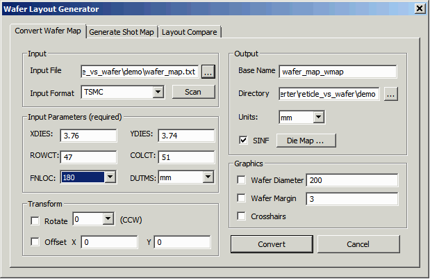
Select a base name for your layout file and a directory where to place it. Now, press the Convert button and a GDSII layout will be created and loaded into Qckvu3 for display. You should see something like this:
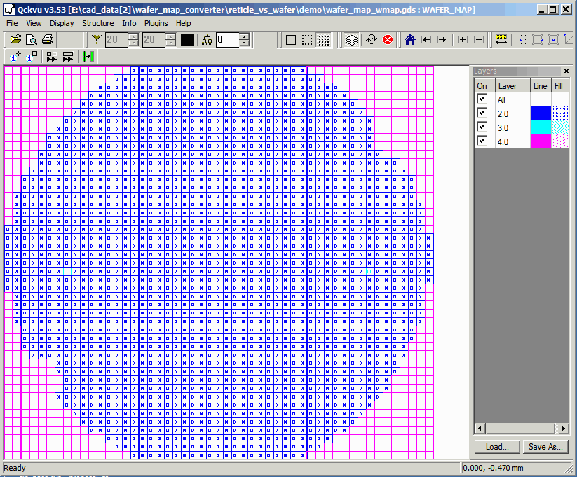
Each die is represented as a rectangle and a text entity for easy identification. It is placed as a cell. This would be an excellent template for our RDL mask with one exception -- we've autocentered the array about 0,0 but in practice the array of die is not placed exactly in the center of the wafer. We need to offset it a small amount in order to precisely match the position of the existing devices on the wafer.
Unfortunately we are never given the offset in terms of the array center. What we are given is a set of shot map parameters along with the offset of the center reticle from the wafer 0,0 point.
So let's move to the second tab and generate a layout using the shot map parameters.
