
This page summarizes the changes, enhancements and fixes to the WMVU program.
Added the ability to flip the wafer horizontally, or vertically. Supported in WMEdit/WMVU via menu/toolbar and in WMBatch via new documented commands.
Facility_id parameterAdded new feature which reads the Facility_id parameter from G85 to support writing to the FACILITY parameter in WWF.
Added an input variant to the TEL(P-12) parser to force die result flag values to override bin value and also read bin quality.
Fixed a bug in the SECS-EG parser related to reading a mismatched byte count.
A new customer requested support for a text based map file format we are going to call E-MAP (we don't really know the software or prober that creates this format) Note that we wrote the reader based on a single sample of this map file which is not best practice but it is all we had to go on.
The format looks like this:
WAFERID = XXXXXXXX.XX
TESTDATE = 2020/01/01 12:00:00
TESTLOC = ZZZZ
DEVICE = XX00000
FABLOTID = XXXXX123456789
WAFERLOTID = X0000
WAFERUNITS = inch
WAFERSIZE = 6
DIEUNITS = microns
XDIESIZE = 4392.0
YDIESIZE = 7011.0
COLCT = 33
ROWCT = 19
FNLOC = 0
BINTYPE = ASCII
BIN = 1;COUNT =     354;STATUS = PASS;DESCR = GOOD (Category = 00)
BIN = A;COUNT =      78;STATUS = FAIL;DESCR = BAD (Category = 00)
BIN = Z;COUNT =       1;STATUS = FAIL;DESCR = BAD (Category = 26)
BIN = +;COUNT =       0;STATUS = FAIL;DESCR = SKIP
BIN = -;COUNT =      73;STATUS = FAIL;DESCR = INKED
BIN = .;COUNT =     121;STATUS = FAIL;DESCR = NO DIE
BINLIST = {
............----A----............
.......---A111A1AA11111---.......
......-1111111A11A1111111--......
....--1111111111111111111AA--....
...-A1111111111ZA1111A11111A1-...
..-111111111111A1111A111111111-..
.-AAA1111111111AA1111111111111--.
--AA1A11111111A11AA11111111AA11-.
-11AAA11A1111A1A1111111A1AA1A1A--
-1111111111111111A111111111111A1-
-11A11111-11111A-11111A111111-11-
--1A11111AA1111A11111111111111A--
.-A11111111111A111A11111111A111-.
.--A11111111111111111111111111--.
..-11AA111111A11AAA1111111111--..
...--AAA1111111111111A111A11--...
....--1A11A1A11-11111A11111--....
......--11111A11111111A1A--......
........---A1A111AA1AA---........
}
Fixed a parsing error when a map file defined the space character (0x020) as the null bin.
UF-3000 allocates 9 bits plus a sign bit to define array coordinates. For a wafer with more than 512 rows or columns one can get an overflow in the count into the 10th bit; a location not allocated to the coordinate position. The UF-3000 reader has been updated to check this overflow bit; this allows row/column range up to 1023. You must set the INPUT_VARIANT=2 in the UF-3000.txt file located in the WMConfig directory to enable this behavior. [Reported by pSemi and found so far only in UF-3000 files submitted by them]
Fixed our interpretation of the array origin location and the direction of increasing X and Y. Previous versions may have displayed a mirrored image of the die locations for the wafer. [Reported by pSemi]
Fixed the G85 writer so that it writes the correct attribute to identify a bin format of HEXADECIMAL-4.
We were recently presented with a SEMI E-142 file where the bin code was defined as ASCII with 6 characters. Added support for the DECIMAL-6 bin format for SEMI-E142 wafer maps.
We recently ran across a G85 map file that used Integer2 (which we are calling Hexadecimal-4) bin codes which we did not support. This has been added to the list of supported bin code types.
We fixed a bug reading MAP 001 format files reported by a customer.
Customer reported a bug in reading a SECS/EG binary map file. Fixed a bug that corrected this.
Added support for reading/writing the new BEIJING wafer map format.
Support for ASCII files encoded using UTF-16 (instead of UTF-8) is now supported.
revised for consistency with WMEdit.
Added support for a rectangular wafer map geometry. There is now a control in the Wafer Map Properties grid, to select the wafer map shape, which can be circle (the default), or rectangle. This setting is only used for visualization purposes.
Modified/improved the automatic wafer center calculation algorithm.
This version improves the parsing of UF3000 files. In addition to the pass/edge/fail flags in the wafer map die results, the new version now also reads the category data and interpret it as a bin code. This allows more differentiation, primarily among the fail devices.
Modified the TEL(P-8) parser so that if more records are found in the file beyond the 1 byte record count data field, those records will be read and
added to the wafer map. This is helpful when the number of records exceeds 256 entries, which is the maximum allowed for the TEL(P-8) spec.
Modified the TEL(P-8) writer so that if the number of contiguous devices is
larger than 255, multiple records will be written to ensure that the
maximum device count for each record does not exceed 255.
Added a new menu item: Edit > Delete NULL Rows/Columns. This feature will remove all rows and columns containing only NULL devices from the outside of
the wafer map.
The core issue was several different sparsely populated wafer files we received which caused problems for the code which calculates the apparent wafer center based on the array. Specifically, we encountered wafers with:
A new algorithm which examined only the non-NULL rows and columns of the array was developed. Rather than using the existing approach for calculating the apparent wafer center, which tried to calculate the centroid, a new method which estimates the wafer center based on bisectors was tested i.e. using the standard approach for determining a circle center based on three points along its curve:
Linear Algebra: Finding an equation of a circle that passes through three points (via Mathematics Stack Exchange)
The algorithm first identifies devices along the wafer edge by looking at the first and last non-NULL device on each row. These devices are then ordered in a radial manner. The [col, row] position of each edge device is treated as Cartesian coordinates. Three devices at a time are used to estimate the wafer center in this way. By selecting non-adjacent devices, the accuracy of the method is improved. And by iterating over all edge devices an average center is calculated. This proves to be very accurate.
Examples of Centering with New Algorithm
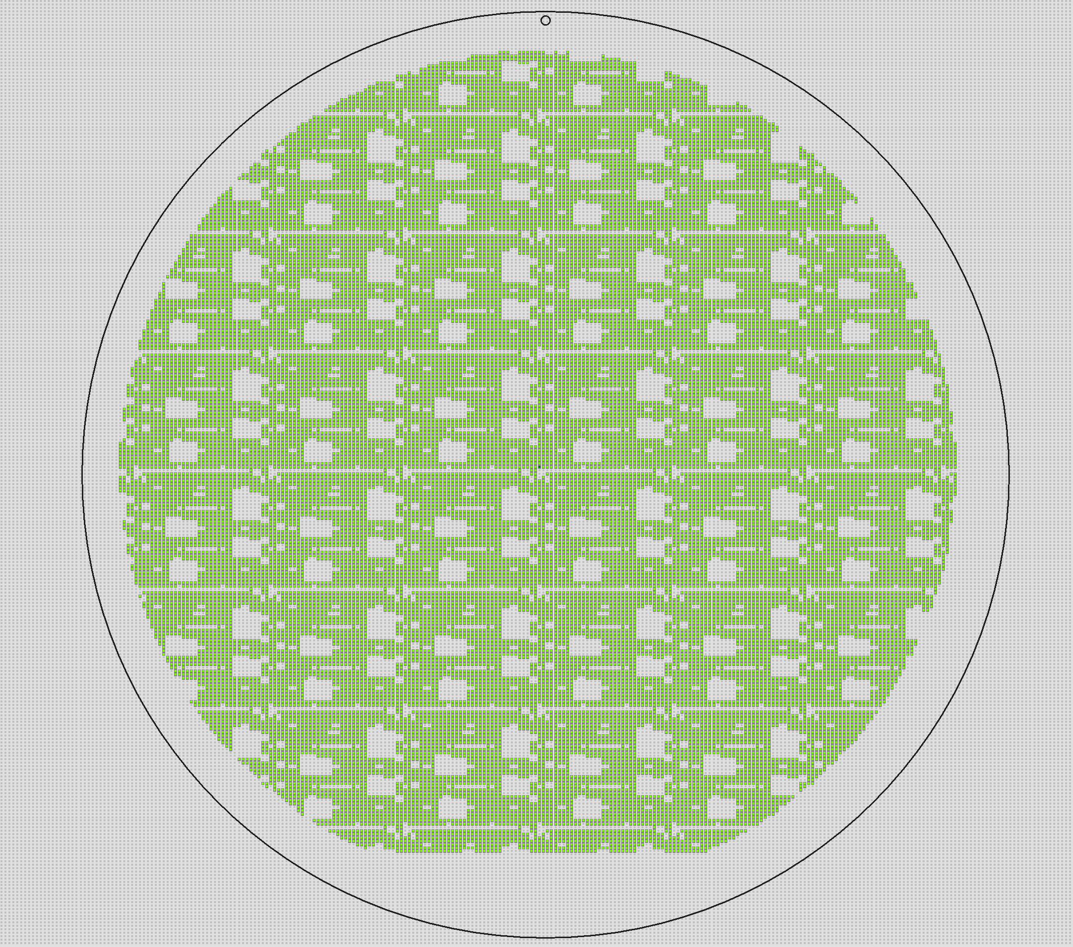
many extra columns on left and right
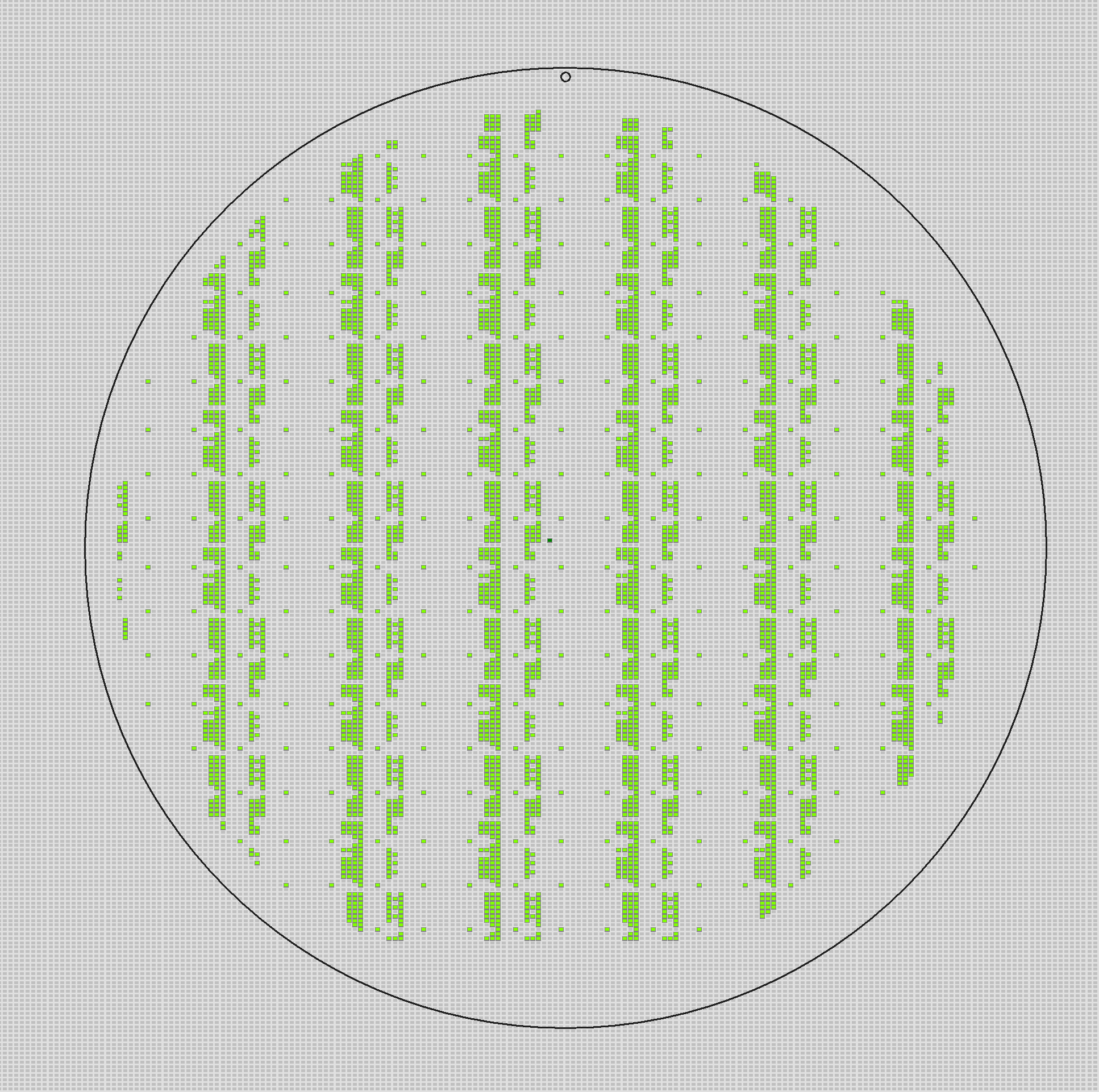
extra rows and columns on all sides; many internal null devices.
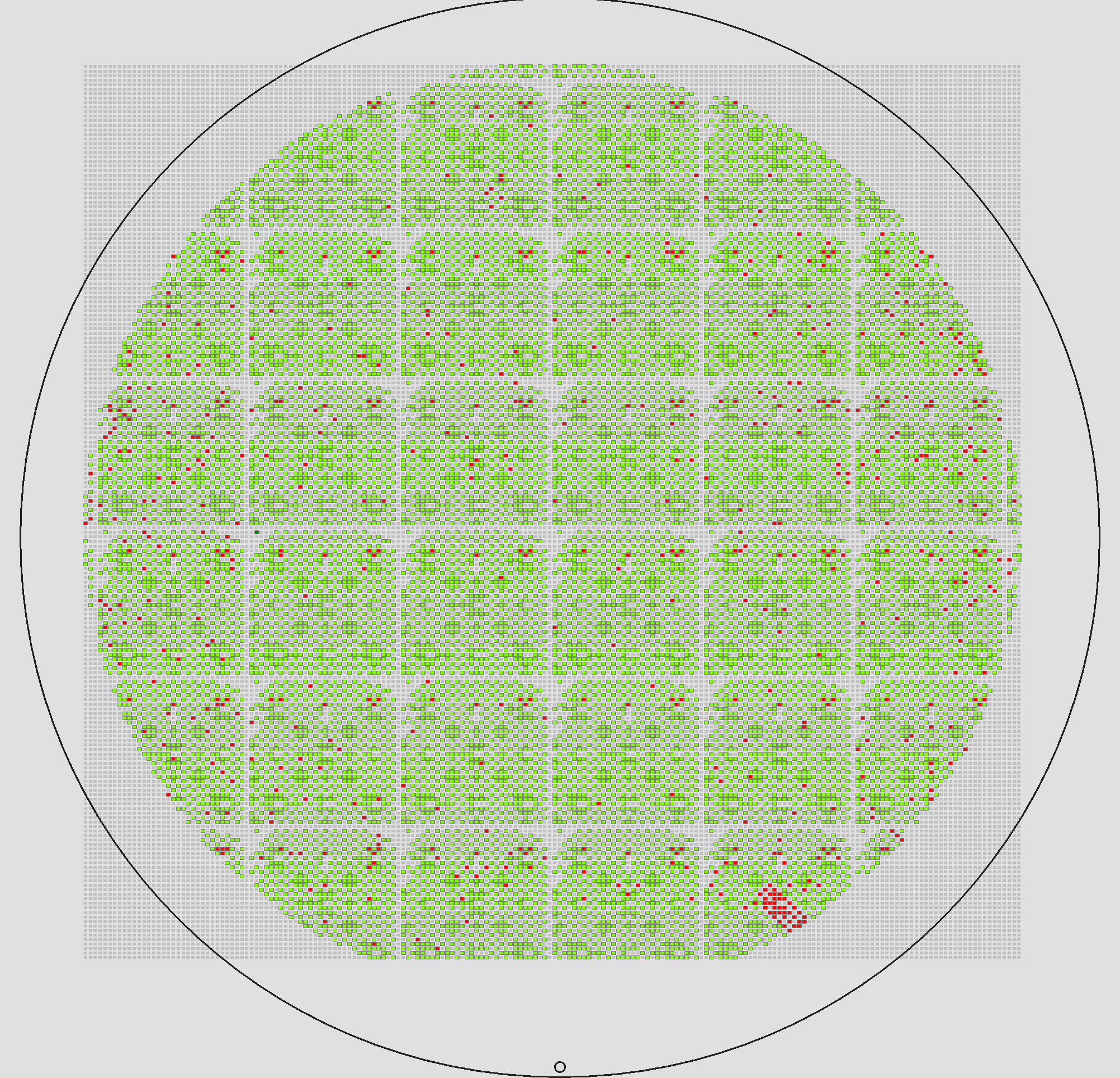
large wafer flat on bottom
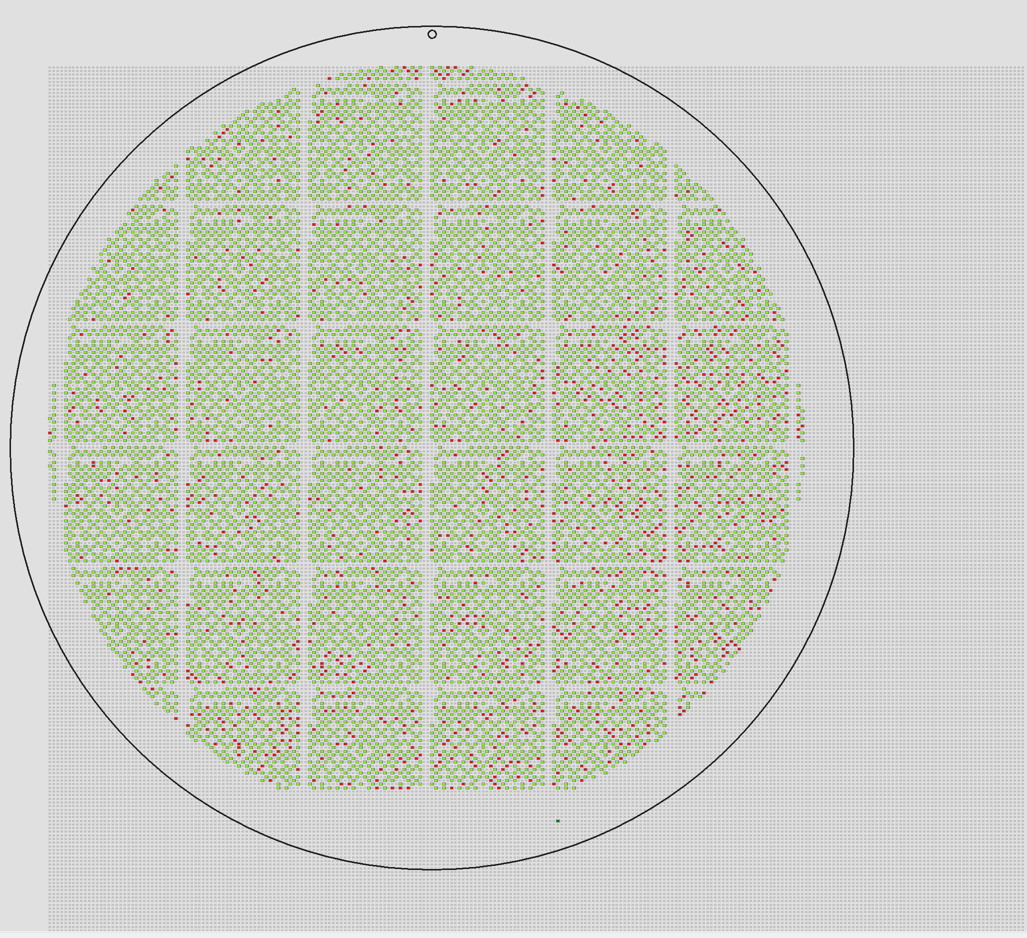
many extra null columns on right and extra null rows on bottom
Partial Wafer Map Files
Finally, for partial wafers, it was necessary to refine the algorithm and ignore devices running all the way across the wafer where one would not expect them (which indicated a partial wafer). This means even if only a quarter of the wafer is present, the bisectors method can still be used to estimate the wafer center. Note that this still works with a sparse distribution:
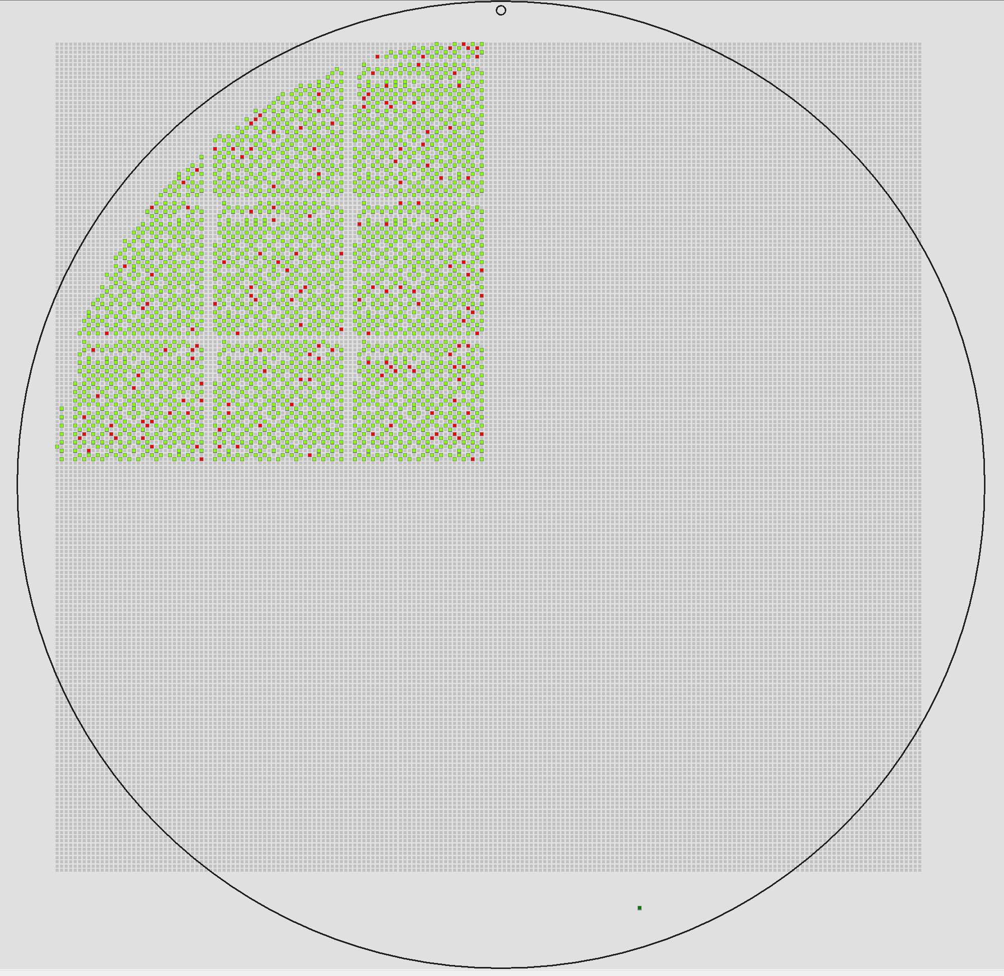
map of upper left quarter of wafer with full array of nulls.
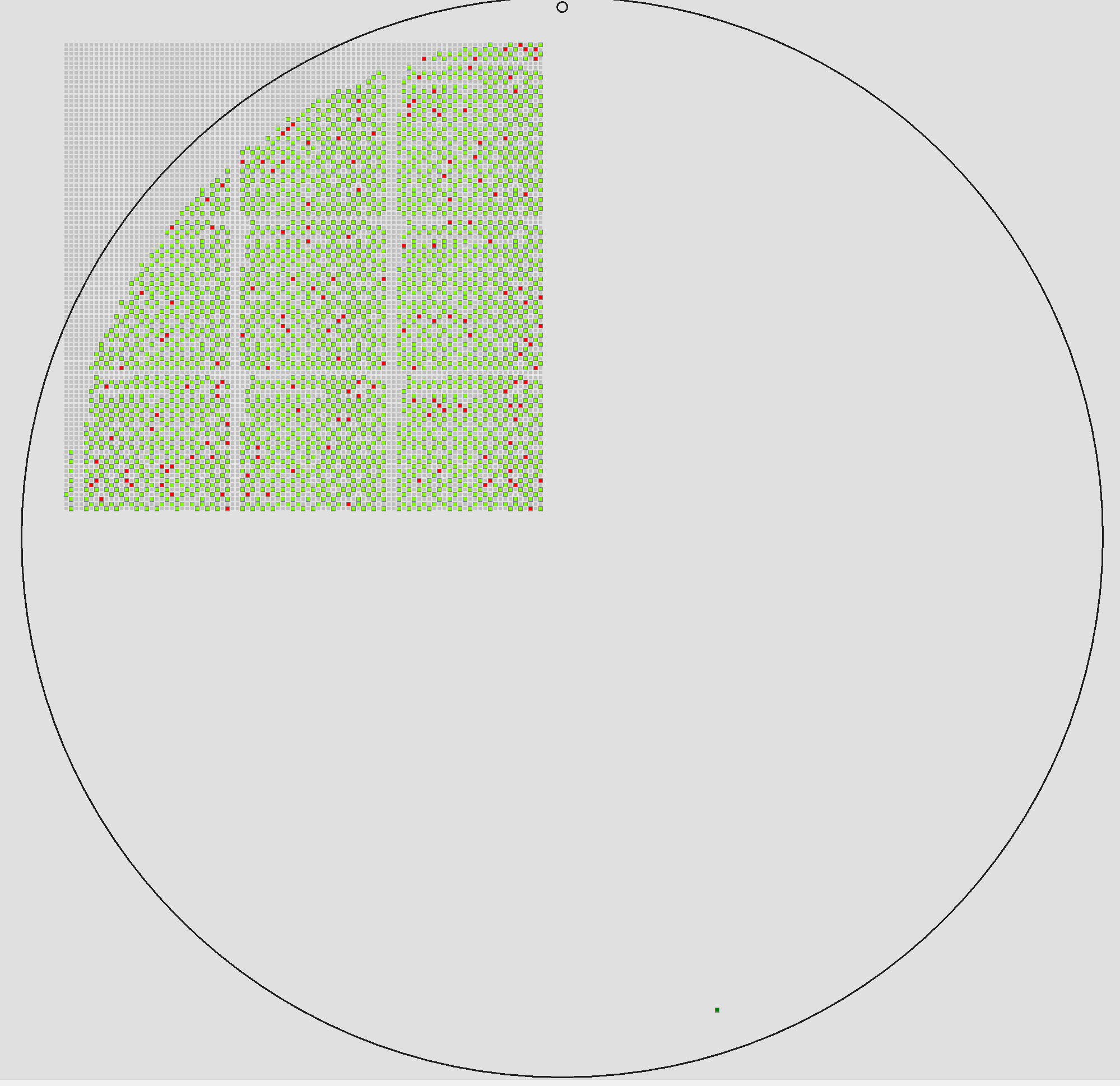
map of upper left quarter of wafer with clipped nulls.
While this new method works very well for these sparsely distributed wafers, we found that it was less accurate for some of the complete wafer files we tested it against. These were wafers which tended to have fewer rows/columns and devices. For this reason, both centering methods are available. The default (Centroid) works best for most wafers. The API also supports the newer method (Bisectors).
To access these options in WMEdit (and WMVU) the new Wafer Outline submenu looks like this:
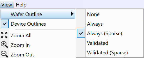
Andrew, the options in this dialog are confusing after reading the prior explanation. You will need to explain these please. (Centroid vs Bisector)
Phantom Devices Displayed
There was a fix in this version to remove the phantom devices reported when viewing a wafer with very large device count and NULL padded rows and columns.
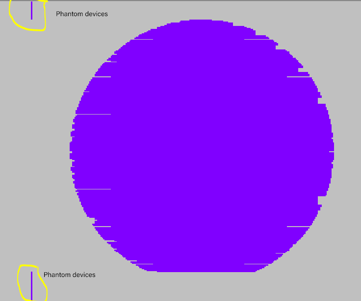
Phantom devices appear for large device count maps with NULL padded rows and columns
The first release of WMVU.