Distortion Correction
Any substrate will expand and contract with changes to its temperature. The amount varies on the substrate material. Some substrates such as fiberglass reinforced expoxies have different coefficient of expansions in X and Y.
Expansion coefficients (CTE) are measured in ppm/C. Typical values for PCB materials range from 10 to 20 ppm/C.
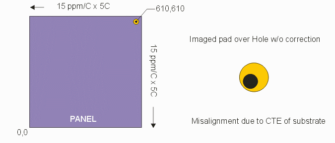
Consider a 610 mm x 610 mm substrate panel that was drilled while it was at a temperature of 30C. However in the lithography room the temperature is 25C. A temperature delta of 5 degrees x 15 ppm/deg = 75 ppm.

For that board the shrinkage would be 75E-6 x 610 mm x 1000 um/mm = -45.8 um
Now this is pretty small number except when you are imaging pads about 150 um in diameter. Misaligning a pad this small by 45 um over the drill hole could result in serious yield issues.
How Much Did Things Move?
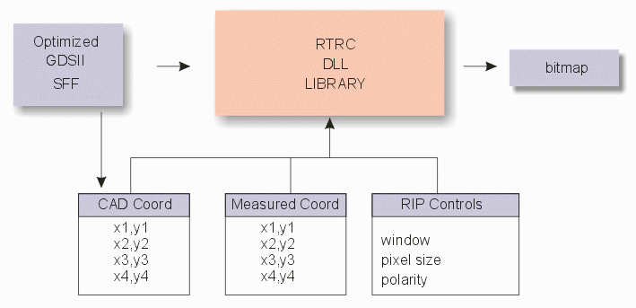
The best way to determine where things are vs. where they ought to be is to actually measure known targets once the substrate is mounted on the image writer. This can be done with down to a micron or better. But what do you do once you have this information?
Correcting the Difference
It turns out that a multi-GByte raster image cannot be easily stretched without creating undesired artifacts. But the vector based CAD data can be stretched or otherwise distorted.
So the only alternative is to input the difference measurements into a fast RIP and rasterize the CAD data just for the panel you have currently loaded into the mask writer.

Rules for Correction Coordinates
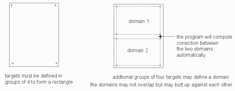
The algorithm used requires correction coordinates to be provided in groups of 4 that form a rectangle.

Correction Available in Preprocessor
Let's say you measure a batch of panels and realize that you only need to make a single correction for the entire batch. You can do it in the SFGEN preprocessor so that it is not necessary to create a new bitmap for each individual panel.
NEXT -> Benchmark of Distortion Correction Timing and Results ...
