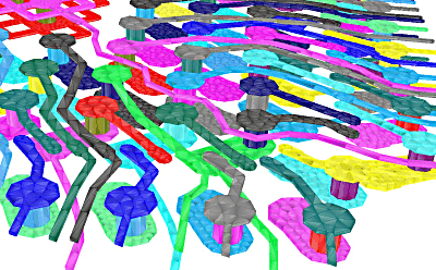

New! Artwork in conjunction with Ansys has developed a new conversion from Artwork's 3Di format to Ansys' EDB (Electronic Data Base). The EDB can be imported into Ansys Electronic Desktop or directly into SI-Wave. This conversion supports conductor layers, vias, dielectric layers, solder mask, components, nets, pins and bond wires. 3Di files generated by Cadence APD/SIP and by Artwork's NETEX-G/ODB are supported.

What if I don't have the Ansys Electronic Workbench?
For users of Ansys's Signal Integrity Products who have stand alone tools and need to import data from a EDA layout, Artwork has developed several tools that greatly simplify this work when a native interface is not available. We can produce either Ansoft Neutral File (ANF) from ODB++ or 3D STEP output from GDSII and ODB++.
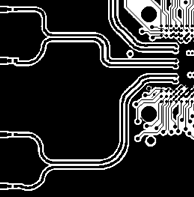
GBRUnion is a useful tool if you have to import a single layer Gerber file into HFSS. Not only does it convert the Gerber data into a clean DXF file, but it also "contourizes" complex Gerber files reducing the number of polygons that are imported into the tool.
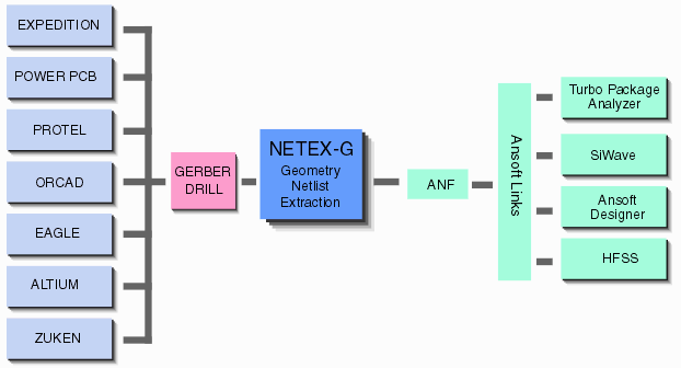
Netex-G is a sophisticated program that takes multiple Gerber files, drill data and stackup information and creates a 3D model of a PCB or IC package. NETEX-G includes a direct ANF output that can be loaded directly into SI-Wave.
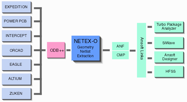
Netex-O extracts conductors, vias, padstacks, nets and components/pins from the Valor ODB++ specification. More detailed board information is available from ODB++ than from Gerber/drill and since all the data comes pre-organized, the conversion is a push-button easy.

All PCB design tools can output Gerber and Drill files as these are used to manufacture the board. Most can also output ODB++ which contains not only the board and drill layout but also netlist and component placement information. This is then formatted into Ansoft's Neutral File which can either be read directly by Ansoft Links or directly by the signal integrity tools such as SI-Wave.
A more sophisticated manufacturing output produced by most PCB layout tools is called ODB++. This format, created by Valor, contains not only all of the conductor and drill geometry but generally includes the netlist and component information. This allows us to produce a more complete output for Ansoft since we can create the cmp file which contains component placement and pin information.

Netex-G for Ansoft - this application note explains how Gerber and drill data from a multi-layer PCB is used to produce an Ansoft Neutral File in order to analyze the electrical properties of high speed differential pair transmission lines ...
