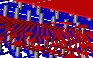

For a variety of purposes, package designers would like to take a stack of Gerber files (or an ODB++ file), and identify and extract all of the metal associated with a particular net or group of nets. Members of the net should be generated by detecting touching or overlapping conductors and vias to build connectivity. Gerber/ODB++ file sets routinely have multiple layers of metal; metal layers are interconnected vertically by vias; small "openings" in the dielectric between the metal layers.

Artwork's NETEX-G program uses Boolean operations to merge connected traces, flashes and polygons into an "electrically" connected set. In addition to the actual Gerber file, NETEX-G requires a technology file that defines the "stackup" i.e. the conductors and vias.
NETEX-G is extremely fast because Artwork is using advanced algorithms developed for the IC world where file sizes are two orders of magnitude larger.
OEM partners who wish to incorporate Netex-G's functionality into their own programs (to support import of Gerber/ODB++ data files) can take advantage of the library version of Netex-G. Special support is supplied to such partners. Contact Artwork for more details.
Describes where in NETEX-G's ASCII output you can find netlist and pin information.
Describes how to extract a netlist from an IC package design (flip chip). The pin labels are imported from an AIF file.
Converting Gerber to clean DXF for import into Ansys/Ansoft HFSS. Includes support for top and bottom solder mask layers. Video link to Vimeo. 05:23 mm:ss