 |
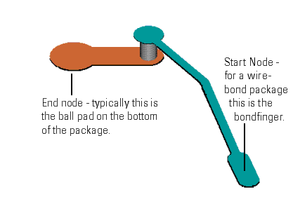
Importing Net/Node Information from ASCIIWhen doing an package analysis it is important to be able to identify each net and at least two points on the net -- the starting point and the ending point. Nets in an IC package are identified by: a netname -- (i.e. clock, IO55, vcc, vss ... however if the package is being analyzed independent of a placed chip there may be no netnames.) a starting point -- where the device connects to the package. This is either a bond finger if wirebonds are used or a bump pad if the device is a flip chip. Bondfingers are usually numbered 1,2,3 ... an ending point - this is the ball pad on the bottom of the package. This is usually labeled with a JEDEC label such as A4, B22, AA15 
|
|
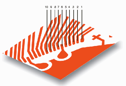
Netex-G can take a net name and a coordinate point anywhere on the net (associated with a particular conductor layer) and identify the net in this fashion. For IC packages such information is generally available -- either directly or indirectly. Direct Coordinate InformationFor wirebond packages the package designer can usually supply a table of bond finger numbers vs. coordinates vs. netnames. This information is required by the package assembler in order to wirebond the chip. NETEX-G can use such a table to assign net names and to label the node on the bond finger. NETEX has an import wizard (much like Excel's text import) that enables the user to identify the row to start importing, and what each column represents (coordinates, start terminal, end terminal, netname) |
|
1 -8641.25 8637.7 2 -8690.66 8461.06 3 -8740.14 8280.14 4 -8781.42 8126.53 5 -8821.55 7973.52 7 -8899.86 7669.11 6 -8861.12 7820.88 8 -8947.94 7473.08 9 -8984.09 7322.75 10 -8435 6816.24 11 -9019.28 7172.9 12 -9054.22 7023.17 13 -9087.7 6874.76 14 -9120.75 6726.61 |

|
|
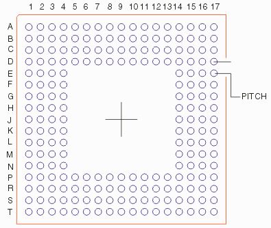
Indirect CoordinatesIt would be nice if we had easily available the coordinates of the ball pads and their labels -- but typically we don't. However it is very common to have the ball pad JEDEC labels and the associated nets. After all, this is how the signal information is passed to a board designer. The JEDEC labels are very useful since they are assigned in a very methodical manner. If you know the JEDEC label and you know the pitch of the ball pads (i.e. the center to center spacing) you can easily derive the pad's coordinates. You still need one coordinate data -- since once does not know the center of the Gerber data. |
|
   A1  vss
   A2  nc
   A3  clock_hi
   A4  scsi[1]
   .   vddio33
   .   scsi[2]
   .   vssio
   B1  pci[1]
   B2  vss
   B3  io55
Package designers routinely supply their customers with a table of JEDEC pad labels vs. the signal name. |

|
Download |
Benchmark Files |
Revision History |
Price |
|
|