PBGA 1
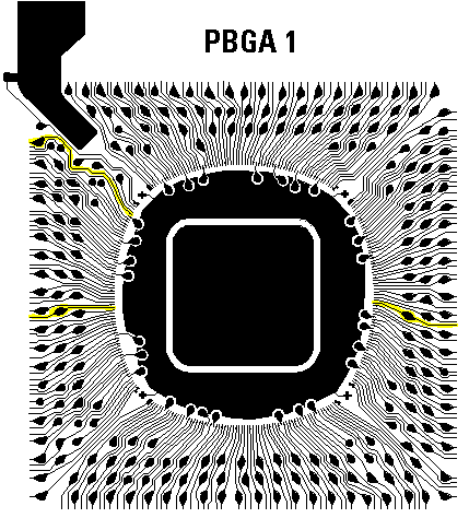
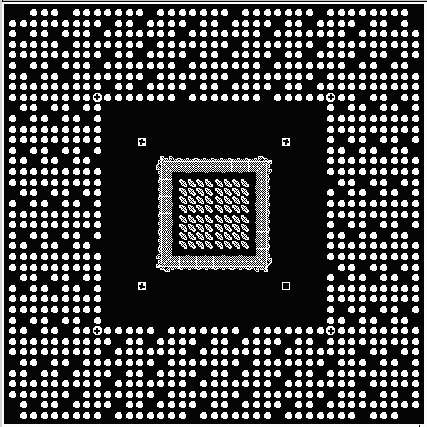
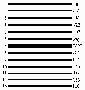
This is a "typical" 2 sided PBGA.
Size: 23x23 mm
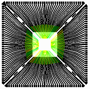
Bondfingers: 280
Finger Width = 100 um
Finger Pitch = 150 um
Via Drill = 200 um dia
Via Pad = 400 um dia
Suggested Nets to Extract:
metal layer = top.gbr
long_1 @ 6.7,17.135
short_2 @ 5.685, 12.245
antenna @ 19.90, 12.939

     Gerber files provided for the extraction:

       Gerber File                    Function
       -----------                    --------
       wbond.gbr                      wires
       top.gbr                        top metal
       drill.gbr                      via
       btm.gbr                        bottom metal
A short tutorial on using NETEX-G to extract the nets of the PBGA with output format of GDSII. (GDSII is useful for IC designers who wish to import the package design into their IC layout and verification tools.
95 KB zip file; requires password to unzip. Gerber files for the PBGA1 tutorial. If you would like to use these Gerber files to test NETEX-G please email artwork for the unzipping password.
A short tutorial on using NETEX-G to extract the nets of the PBGA with output targeted to Ansoft's Neutral File (ANF).
94 KB zip file; requires password to unzip. Gerber files for the PBGA2 tutorial. If you would like to use these Gerber files to test NETEX-G please email artwork for the unzipping password.


