 |
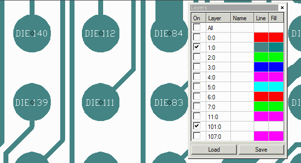
GDSII Node TextA GDSII file created from a PCB source should have a way to label the various pin names and locations. Such a label does not exist natively in GDSII so we use a layer of text to hold this information. Encoding Schema The basic encoding schema is fairly simple. We assume that nodes are associated with a conductor layer. Typically this is the top and bottom layer (though it need not be) We generate a string of text based on the pin's name and reference designator. For example, if you have a pin labeled 5 and it is attached to a component whose reference designator is U1, then the string of text will be U1.5. This is consistent with most PCB conventions. We place the TEXT string at the location that corresponds with the physical location of the pin center from the PCB database. We place the TEXT string on a layer that is offset (by a user specified value) from the conductor layer associated with that pin. For example, if the component is mounted on the "TOP" side of the board and that layer = 30, and the use specifies an offset for node text of 100, then we will place all pin labels associated with the top side of the board on layer 130. Example In the snapshot below you can see that the top GDSII layer of a flip chip (exported from package design software) is on layer 1. The node text offset was set to 100 so the node labels for the top appear on layer 101. You can see that each "bump" pad which is effectively a pin on the DIE symbol is labeled with a string of text.  The text height is user controllable and the text insertion point (the small diamond) coordinate matches that of the source pin. The text is justified center-middle. |
Download |
Benchmark Files |
Revision History |
Price |