|
| |
Layer Stackup Dialog
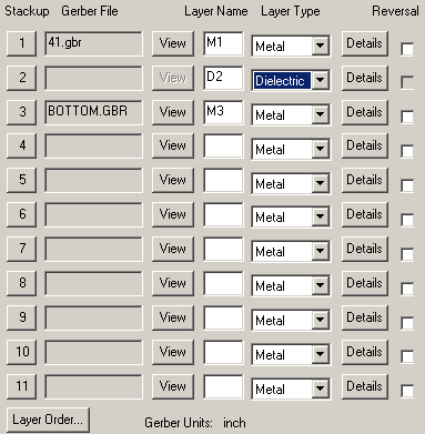
The first step in running NETEX-G is to define the layer stackup. This dialog is present in the main menu of NETEX-G.

Stackup - the numbers in the button indicate the stackup position. Remember the top of the substrate starts at 1. Pressing this button will open the dialog box for selecting a Gerber file.
Gerber File - the Gerber file that defines the geometries for this layer. Dielectric layers do not have a Gerber file associated with them.
View - once a Gerber file has been selected, the view button launches GBRVU so that you can visually inspect the file.
Layer Name - an arbitrary name you assign to this layer. A typical approach is to define the conductor layers as M1, M2 .... depending on their order in the stackup.
Layer Type - select from the drop done one of the following: metal, dielectric or wirebond.
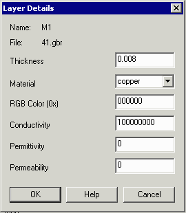
Details - clicking on the Details button opens another dialog that enables you to enter the layer's thickness, material and electrical properties. It is not necessary to do so for proper execution of NETEX-G but if you do, the data you enter here will be passed to the ASCII output.
Reversal - sometimes the board designer outputs the reverse polarity Gerber -- especially for power and ground planes and for soldermasks. If you have inspected your Gerber data and determine that a layer is reversed, check the reversal button and NETEX-G will properly recognize which areas are metalized and which are empty.
|


