web_page_logo.gif


More Map Formats

Here are some more map formats we've run across but don't necessarily support at this time. However we are constantly examining the demand for such formats and will add them as our user's requirements dictate.


No Header

This file consists solely of the row and column bin codes. It appears that "." is used for the null bin, and various digits (1-9) for other bins. Based on the pattern it appears that "7" marks edge die, "8" is not on the edge but near it (no way to know whether it is counted as good or bad), "9" represents good die and "1" represents bad die. All the other information one would expect in a wafer map must somehow be transmitted separately.

Header

NONE

Row Data

Row data lines look like this:


.....................................777777777777777777777777777.....................................
...............................777777788889999999999999999988887777777...............................
...........................77777888999999991199199999111199999999988877777...........................
........................77778899999999999991991199991919919991919999999887777........................
.....................77778899999999991999991199199911991119991999999999999887777.....................
...................777889999991199999199999919199919191191999991999999999999988777...................
.................7778999999919119119991999999999991999999919999999999999999999998777.................
...............77789999991911911911911919999999999991191199119999999999199999999998777...............
.............777899999911919911199919199999999999999991199191999999991919999999999998777.............


Non Standard Header

This file has all the required header information plus a lot of information probably specific to the tester, but the header certainly does not adhere to any industry standard nor does the row and column ID.

Header

WAFER_MAP = {               --> starts here
WAFER_ID = "XXXX0.0.X-00"   --> standard wafer map parameter
MAP_TYPE = "ASCII"          --> may be other options
NULL_BIN = " "              --> not really helpful   
ROWS = 169                  --> number of rows in map array
COLUMNS = 122               --> number of columns in map array
FLAT_NOTCH = 180            >-- might be top or bottom
X_FIRST_REF = 40            >-- X position of a reference die
Y_FIRST_REF = 158           >-- Y position of a reference die
X_SECOND_REF = 83           >-- X position of a reference die
Y_SECOND_REF = 158          >-- Y position of a reference die
SUPPLIER_NAME = "XXXX"      >-- only useful if target format supports supplier
FORMAT_REVISION = " "       >-- not used
DEVICE = XX000XX-X-XXXX     >-- device ID
LOT_ID = XXX0.0.X           >-- LotID
STATUS = XX0                >-- not used
PROBE_DATE = 20160130       >-- not used
WAFER_SIZE = 200            >-- dia in mm (even though units declared to be um)
X_SIZE = 1640               >-- die pitch along X; 
Y_SIZE = 1176               >-- die pitch along Y;
REF_DIES =2                 >-- number of reference die
REF_DIE =                   >-- name assigned to ref die
TEST_TEMP = 30              >-- not needed
UNITS = "MICRONS"           >-- distance units
FILE_TYPE = "WMAP"          >-- 
FILE_VERSION = " "          >-- 
BINS = 2                    >-- number of bins
BIN = "P" 14627 "PASS"      >-- bin definition
BIN = "F" 198 "FAIL"        >-- bin definition
DIES = 14825                >-- number of die tested?
MAP = {                     >-- start of map

. = null bin
* = edge die
F = fail
P = pass
+ = reference die

A portion is shown below

..............................************************************************........
.............................******FFFPPPPPPPPPPPPPPPPPPFPFFFPPPPPPPPPPFF******........
...........................******PPPPPPPPPPFPPPPPPPPPPPPPPPFFPPPPPPPPPPPPPF******.......
..........................*****FFPPPPPPPPPPPPPPPPPPPPPPPPPPFFPPPPPPPPPPPPPPPP*****.......


Unintelligible Header

This file has a 4 line header but the the data seems intended to identify the wafer. I've substituted the actual characters/numerals for arbitrary ones but even the original values supplied by the client don't tell you anything about the wafer or die.


Header

XXX
X0X000.0X
X0X000.0X-00
X0X00000.XXX

Map Data

. = null bin
X = edge die and bad die (most files differentiate between the two but not here)
1 = good die


............................XXXXXX.....................................
.....................X111111X11111X1X11X1X.............................
.................11111111111X11111X11X1111XXXX.........................
..............X11111111111111111X111111111X111X1X......................
...........1111XX11X111111111X11111111111X111X11111.....................
.........11111111111111X1111111111111111111111111111X...................
.......X1111111111111111111111111111X1111111111111111XX.................


XML IBIS

This is an XML format (identified as IBIS at the beginning).


<?xml version="1.0"?>                           
<IBIS_WAFER_DATA>                                      identifies as an IBIS wafer data
<HEADER>                                               start of header section
<WAFER_OCR_ID>TESTW07F1</WAFER_OCR_ID>                 wafer ID - OCR readable on wafer/frame
<WAFER_BATCH_ID>TEST</WAFER_BATCH_ID>                 
<WAFER>07</WAFER>                                      wafer number 
<PRODUCT>TYPE1</PRODUCT>                               product ID 
<DEVICE>DEVICE1</DEVICE>                               Device identification
<XSTEP>1.153000</XSTEP>                                X stepping (units in mm??)
<YSTEP>1.153000</YSTEP>                                Y stepping (units in mm??)
<FLAT_LOCATION>90</FLAT_LOCATION>                      flat is on left side
<FLAT_TYPE>N</FLAT_TYPE>                               guessing that N = notch
<XREF></XREF>                                          don't know
<YREF></YREF>                                          don't know
<XDELTA>0</XDELTA>                                     don't know
<YDELTA>0</YDELTA>                                     don't know
<PRQUAD>1</PRQUAD>                                     probe quad start
<COQUAD>1</COQUAD>                                     coordinate quad reference
<DATE>11-10-2016</DATE>
<TIME>12:01:00</TIME>
<DIFF_CTR_ABR>XXX</DIFF_CTR_ABR>                      don't know
<PROBER>MAPWIZARD_1.7.1.1</PROBER>                    prober/software used to generate
<CEPT_12NC>NO_CEPT</CEPT_12NC>                        don't know
<SLDI_12NC>NO_SLDI</SLDI_12NC>                        don't know
<FIRST_DIE>29,33</FIRST_DIE>                          array position of first die probed?
<XOFFSET>143</XOFFSET>                                don't know
<YOFFSET>33</YOFFSET>                                 don't know
<BIN_COUNT_PASS>19634</BIN_COUNT_PASS>                count of die that passed
<WAFER_SIZE>200</WAFER_SIZE>                          wafer diameter
<WAFER_UNIT>MMT</WAFER_UNIT>                          units of wafer
<BIN_CODE  
 PASS="1" 
 PASS_2="2" 
 OTP="3" 
 IREF="*"       
 OPTICAL_PASS="?" 
 UGLYDIE="/" 
 EDGEDIE="-"                  
 SKIPDIE=":" 
 BIN206="?" 
 BIN205="?" 
 bin53="]" 
 BIN59="?" 
OPTIREJ=";" 
OUTSIDE="." 
>
</BIN_CODE>
<COLUMN_COUNT>171</COLUMN_COUNT>                      number of columns in the matrix
<ROW_COUNT>171</ROW_COUNT>                            number of rows in the matrix
<DIE_SPACING_CX>0</DIE_SPACING_CX>                    don't know - street?
<DIE_SPACING_CY>0</DIE_SPACING_CY>                    don't know - street?
</HEADER>

After the header section comes the XML markup:

<WAFER_MAP>

which is followed by an continuous "stream" of ASCII bin codes with no spacing. It is the responsibility of the reading software to break these into chunks of 171 codes per row since that is the declared row width.

the stream of bin ID's is terminated with:

</WAFER_MAP>
</IBIS_WAFER_DATA>

The stream of bin ID's sums to 29,241 characters so this matches the array size of 171 x 171.


Cascade PA200

The Cascade Microtech .map file is an ASCII text file containing various sections including:

    [Header]
    [Wafer]
    [Bin]
    [Die]
    [Process]

It has an unusual map structure. Instead of reporting the bin codes in a 2D array it merely lists their order in the array -- but one has to know the "path" that the prober follows in order to associate the die with its correct position in the array.

The Header Section
[Header]
Description=Wafer Map File
Version=1.3
[Wafer]
Revision=0.0
Diameter=70
FlatLength=15.9
FlatAngle=0
EdgeArea=0
XIndex=10000
XOffset=0
YIndex=10000
YOffset=0
Shape=Wafer
DieInX=7
DieInY=7
Origin=UL
DieMapStyle=Single
HomeDie=1,1
RefDieOffset=0,0
UseClusters=0
ClusterSizeX=1
ClusterSizeY=1
TestFrom=2
TestFaulty=0
RouterStartColumn=Left
RouterStartRow=Top
RouterType=HorSingleDir
  The Bin Section
[Bin]
0=1,a0,00C000,1,0,0,0,0
1=1,a1,0000FF,0,0,0,0,0
2=1,a2,FF0000,0,0,0,0,0
3=1,a3,FFFF00,0,0,0,0,0
4=1,a4,FFFF80,0,0,0,0,0
5=1,a5,808000,0,0,0,0,0
6=1,a6,00FF00,0,0,0,0,0
7=1,a7,00FFFF,0,0,0,0,0
8=1,a8,C0FFFF,0,0,0,0,0
9=1,a9,8000FF,0,0,0,0,0
10=1,b0,FF00FF,0,0,0,0,0
11=1,b1,800080,0,0,0,0,0
12=1,b2,FF0080,0,0,0,0,0
13=1,b3,008080,0,0,0,0,0
14=1,b4,000080,0,0,0,0,0
.
.
.
248=1,V6,FF00D2,0,0,0,0,0
249=1,V7,FF00D8,0,0,0,0,0
250=1,V8,FF00DE,0,0,0,0,0
251=1,V9,FF00E4,0,0,0,0,0
252=1,W0,FF00EA,0,0,0,0,0
253=1,W1,FF00F0,0,0,0,0,0
254=1,W2,FF00F6,0,0,0,0,0
255=1,W3,FF00FF,0,0,0,0,0
  The Die Section
[Die]
0=X
1=X
2=X
3=X
4=X
5=X
6=X
7=P
8=P
9=P
10=X
11=X
12=X
13=P
14=P
15=P
16=P
17=P
18=X
19=X
20=P
21=P
22=P
.
.
.

More details are available here ...


Binary Map Formats

Unless one has documentation from the binary file creator, it is very difficult to extract useful information from just a sample file.

However in one case we were able to reverse engineer the map data (though not all the other data as we did not have the encoding information)

The file has a name in the form: wafer.dat

When we examined it in a hex editor we see something like this:
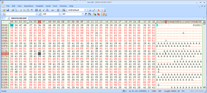
hexedit_of_binary_file.gif

Other than some ASCII text in the beginning there's not much to see except some repeating values that are likely the die ID's in some sort of array. After some educated guessing and experimentation we were able to extract that section of the binary file and convert it into an ASCII equivalent which I show at full screen below:
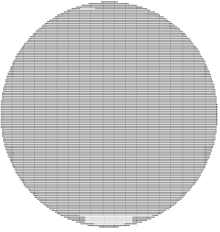
binary wafer map converted into ASCII and displayed in Word (adjusted the line spacing to get a nice square image)

and here are a few of the top rows where you can see the edge die (N) the good die (A) and the knocked-out die (-).

zoomed in view where one can see the edge die, good die and knocked out die


Electroglas Prober

We received a pair of files that originated from an Electroglas EG-1 prober.

Header File

I've added carriage returns to make the data more man-readable. Annotations in italics are mine.


4                        no idea what this is
diameter=200000,         wafer diameter, 200,000 um
refDieOffsetX=0,
refDieOffsetY=0,
dieSizeCX=1835,          die size X units look like um
dieSizeCY=2979,          die size Y units look like um
dieSpacingCX=0,          maybe a street width?
dieSpacingCY=0           maybe a street width? missing comma?
flatOrNotch=1,           presence of a flat or notch (1=true 0=false?
FlatAngle=0,             maybe 0=bottom?
UseSecondaryFlat=0,
secondFlatAngle=0,
numRows=73,              number of rows
numCols=115,             number of columns in map array
orloc=4,
praxi=1
NullBinCode=255,
MCSVectorX=57,
MCSVectorY=36,
MCSFactorX=-1,
MCSFactorY=-1,
RefDieX=0,
RefDieY=0,
numBinGroup=15            number of bin groups to follow

Now its not entirely clear what is going on below. The descriptions make
sense; the values ranging from 0-255 imply that the binary file is using a full
byte to identify each device.

What is not clear is the meaning of the first large number e.g. 16579836

Unused_Bingroup ,16579836,0,101,200-250,255,None
Good_Bingroup   ,3182592,1,GOOD
Good1_BinGroup  ,3182592,100,GOOD                   Hex=64
OS_Bingroup     ,7111856,2,BAD                      Hex=02
OS2_Bingroup    ,7111856,102,BAD                    Hex=02
PAD_Bingroup    ,5263520,3-5,BAD       
VDD_Bingroup    ,9449616,6-7,BAD       
IDDQ_Bingroup   ,33020,11,BAD                       Hex=0B
IDD_Bingroup    ,49344,12-13,BAD
Bad_Bingroup    ,3158204,8-10,14-99,BAD
Bad2_Bingroup   ,3158204,103-199,BAD
Edge_Dies       ,6303744,254,None                   Hex=FE
Edge_Parallel   ,10521680,253,None                  Hex=FD
Clamp           ,49344,252,None                     Hex=FC
Flat            ,11053224,251,None                  Hex=FB

      
WaferID=A99999-99-A9,      I've obsfucated the real Wafer ID but 
ProdId=Aaaaaaaa Aa9/Aaa,   numerals and characters/case are preserved
LotID=A99999,OPID=9,
TSID=9,TSIP=Aaaaaa,
DeviceID=
ProbeCardID=AA9999.99,
ProberName=EG-1,
LoadBoardName=,
LotRcpID=LR_Probe,
WafRcpID=WR_Probe
GoodCount=4886,
BadCount=430,
UglyCount=0,
TouchDown=176981,
ProductSource=Remote Drive,
TesterMsg=
FirstDieX=-9,
FirstDieY=32,
FirstDieBin=2,
SCXRefOffset=372,
SCYRefOffset=-211,
WaferStartTime=20160606.094448,
WaferEndTime=20160606.202125

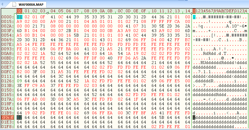
and now on to the binary map data. The file suffix ends in .MAP. The data is binary.

binary_hex_of_electroglas_map_file.gif

I've greyed out the Wafer ID but it matches what we found in the .XTR file

If we assume that 255 (FF) is a placeholder for no die, and 254(FE) is edge die as it appears from the header then we would expect to see FF followed by FE on the left and then again on the right.


Download Revision History Video Tutorials Price