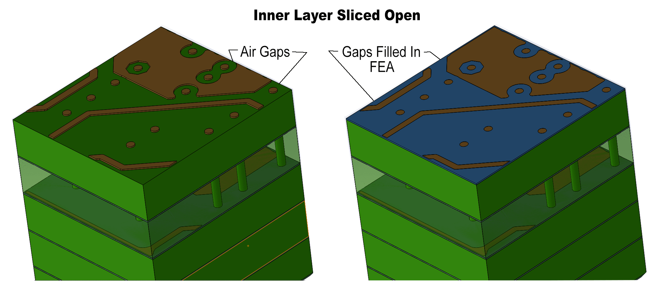
Designers who need to perform thermal or stress simulation in SOLIDWORKS have a number of special requirements that those who are doing form-fit-function do not need to consider. In the notes below we will describe what the optional Thermal FEA does to improve simulation.
The standard version of Read3Di treats each conductor layer and each dielectric layer independently. While this is fine for applications such as form-and-fit, it causes problems for simulation.
Why? The "air" gaps and spaces on the conductor layers generate discontinuities that can cause a simulator to fail or generate bad results.
When a multi-layer PCB is manufactured, the boards and prepeg are placed into a press and heated. The dielectric "flows" into any empty gaps between conductors on a given layer and provides a fairly uniform encapsulation of the conductors.
So how do we deal with this?
The user checks Enable Negative Dielectric.

This activates Artwork's Boolean library which subtracts the conductor layer geometries from a bounding box (normally the package or board outline.) The result is one or more solid bodies that "fill" in the gaps between conductors. These solid bodies are aggregated into a SolidWorks part and placed at the correct height. They serve to fill in all the air gaps. See below:

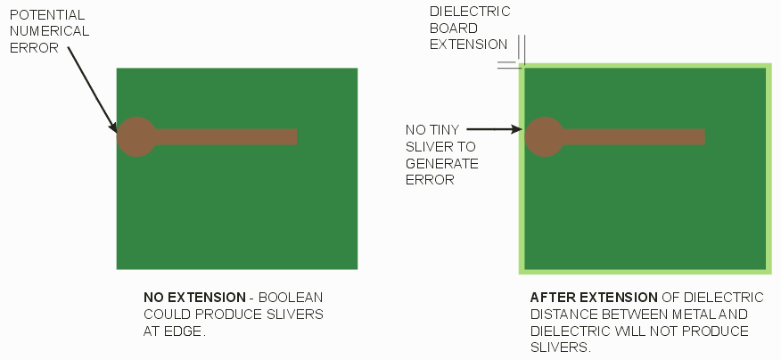
This function is not a a feature as much as a necessity that we discovered when generating the negative dielectric. It may need to be turned on to insure that our bounding box extends slightly beyond any conductor geometry.

The extension insures that the Boolean operation creating the "negative" dielectric regions does not produce tiny slivers. These tiny slivers might not extrude when passed to SolidWorks as sketches and prevent the conversion to 3D.
Enable Drill Holes - insures that the hole in the dielectric is drilled through for the via and that the faces properly match so that there are no tiny gaps between the via cylinder and the hole in the substrate. Any such gaps can cause the mesher to fail.