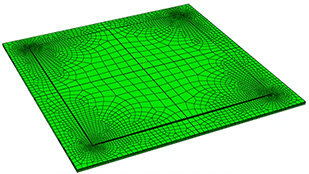
There are many reasons one would want to import a 2D PCB, IC or package layout into SOLIDWORKS as a 3D geometry: checking mechanical interferences in 3D, doing a heat flow simulation, stress simulation or other type of finite element simulation.
Getting EDA data into SOLIDWORKS has been quite difficult if you need copper traces, pads and planes.
Read3Di was designed to address this problem.
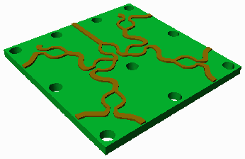
Read3Di is a plug-in -- code that works with SOLIDWORKS via the SOLIDWORKS API. We combine our powerful libraries for conditioning data along with API calls to create sketches, extrude them into solid bodies, then place parts into an assembly to bring in the original 2D data into SOLIDWORKS as 3D data.
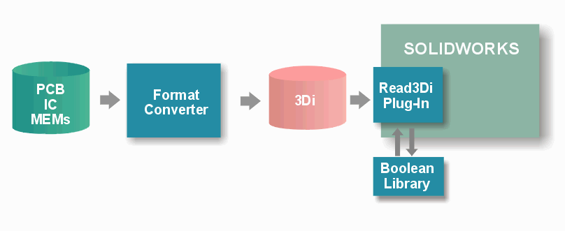
Each 2 1/2 D object in 3Di (a 2 1/2 D object is a 2D planar region with a Z extrusion) is brought into SOLIDWORKS and extruded. When complete, there is an accurate representation of the EDA layout in 3D that can then be used for simulation.
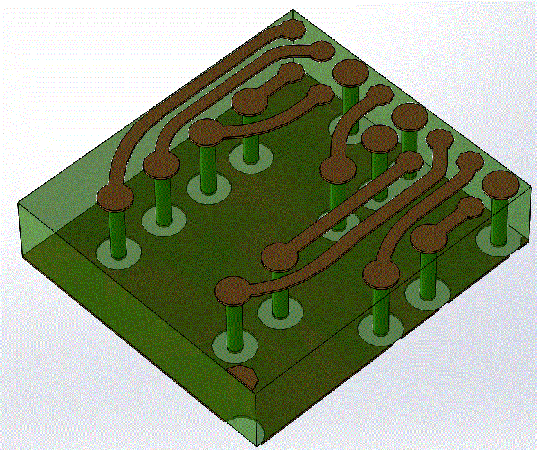
Data Conditioning is Key
The key to successfully importing conductor geometries is in properly "conditioning" the 2D data so that it will extrude into a 3D solid body. The SOLIDWORKS' modeling engine is very particular about the extrusion process and it often rejects sketches that have closely spaced vertices or other small artifacts that are almost invisible. Much 2D data extracted from CAD layout tools suffers from these tiny defects.
Organizing the Geometries
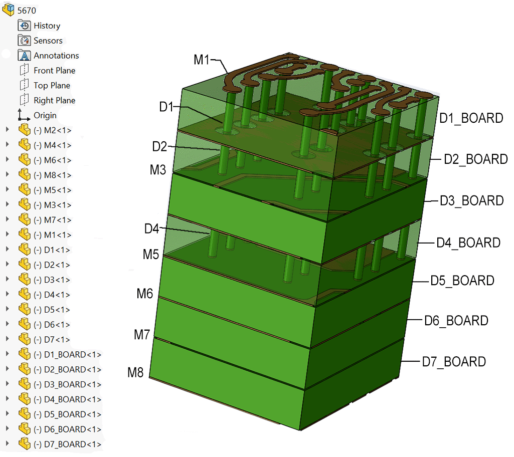
Trying to cram thousands of solid bodies into a single "part" in SOLIDWORKS is generally not useful and not successful. Instead, we group geometries into parts based on a user defined specification. The most common sort is by layer so that all geometries on a given EDA layer are mapped to a part in SOLIDWORKS. However for some simulators it is preferable to group all conductors belonging to a single NET into a part. We can even sort the conductors by net and the dielectrics by layer.
Size Limitations
A 3D database is much more complex internally than a 2D layout database. One cannot expect to be able to import large PCBs or other designs completely into SOLIDWORKS. This is not a limitation of the import plug-in but rather a basic limitation of the underlying database powering SOLIDWORKS.
Because of this constraint, it is common to select only a portion of an entire PCB, IC layout or package layout for importation.
A number of board and package designers are starting to do detailed analysis on their substrates - in particular to model thermal flow through a multi-layer board and to model stresses generated on the vias and conductor layers as a function of temperature.
To successfully perform a finite element based simulation requires additional data conditioning. Artwork has worked closely with engineers doing this type of work - check here for details on what special options we have developed specifically for this application.
