Smart Die Plug InThe Smart Die Plug-In is used by chip and package designers to extract the die pad locations from a GDSII layout and output an ascii file. It runs inside of Artwork's Qkcvu3 layout viewer. One of the first steps in designing an IC package is to create a table of chip pad locations, number each pad and associate each pad with a net or signal name. SmartDie can automate this process using a GDSII layout as input. How it WorksSmartDie works by scanning the pad opening layer and identifying shapes that "look" like die pad openings. It can handle square, rectangular and polygonal die pad shapes and uses a statistical approach to differentiate a die pad from, say, a die outline or logo. It categorizes the shapes into pad stacks (many die have 2 or more differently shaped die openings) and finds their centers. |
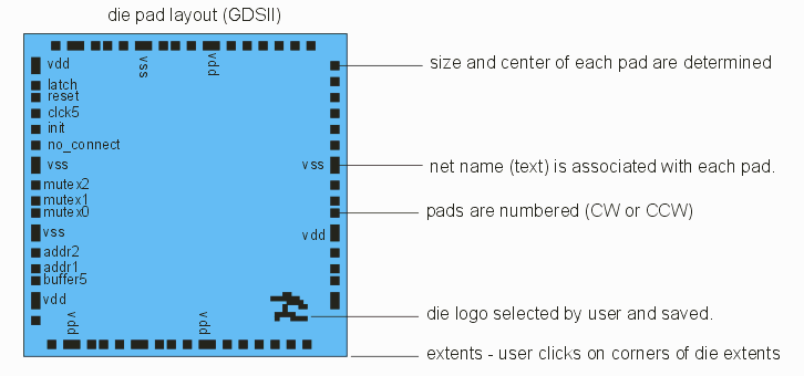
FunctionsDie Pad Numbering - Once the die pads have been identified (and a user can intervene by deleting or adding objects) it can then number thos pads in a clockwise or counter-clockwise direction. It also supports two rows of staggered die pads for numbering. Net Labeling - If the GDSII file has text that has been used to label the die pads, SmartDie can associate each string of text with the "best" die pad and include the net name when creating the output table. It does not require that the text fall under the die pad but it does require that there be the same number of die pads as text entities so that it can assign labels to die pads using a optimization algorithm. Die Logo - The user can select a window and collect the polygons forming a die logo. The vertices of these selected polygons are output in ASCII format. Output Format - The output file is an ASCII table in a format known as AIF. The AIF file can be imported by several package design tools including Cadence APD/SIP and Sigrity's UPD. |
PlatformsLinux (64 Bit OS) Windows XP/Vista User IntefaceLinux Demolinux (flash) FAQlayers net labeling split die pads |
Download | Revision History | Linux Install | Windows Install | Price |
|