web_page_logo.gif


Supported Wafer Map Formats

As we started working with the SINF file format for wafer maps we immediately were provided with a number of wafer maps that did not follow the required syntax. We had to add both new parser routines and also prompt the user for information that should have -- but wasn't -- been present in some of these sample files.


SINF

The SINF [Simplified Integrator Nested Format] spec consists of a header section followed by Row data. The basic structure is shown below:

Header


DEVICE:xxx       identification assigned by originator
LOT:xxx          identification assigned by originator
WAFER:xxx        identification assigned by originator
FNLOC:180        wafer flat position (0=TOP,90=RIGHT,180=BOT 270=LEFT)
ROWCT:62         number of rows
COLCT:63         number of columns
BCEQU:01         List of Bin Codes that are good die
REFPX:           x-coord of reference die (optional)
REFPY:           y-coord of reference die (optional)
DUTMS:mm         die units of measurement (mm or mil)
XDIES:2.945      step along X
YDIES:2.945     step along Y

Row Data

Following the header is row data. It is identified by the keyword RowData: Here are the various hex values one will find in the row data:

00-0A                good die (each die type gets its own unique identifier starting at 00, 01, 02 ...)
                     reserve 0A for the die at wafer center.

0B-F0                bad die

__                   no die (underscore-underscore) used as a placeholder in the matrix.

@@                   uninspected die

FD-FE                edge die (optional)

FF                   reference die (typically a die that is visually different)

Row data lines look like this:


RowData:__ __ __ __ __ __ __ __ __ __ __ __ __ __ __ __ __ __ __ __ 01 01 01 01 __ __ __ __ __ 01 01 01 01 01 01 01 01 
RowData:__ __ __ __ __ __ __ __ __ __ __ __ __ __ __ __ __ __ 01 01 01 01 01 01 01 01 01 01 01 01 01 01 01 01 01 01 01 
RowData:__ __ __ __ __ __ __ __ __ __ __ __ __ __ __ __ 01 01 01 01 01 01 01 01 01 01 01 01 01 01 01 01 01 01 01 01 01 

Reference Die

There are two ways of locating the reference die:

    a) a die marked with bin code FF.

    b) REFPX: and REFPY: values in the header.

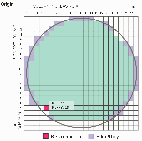
The coordinate system when REFPX: and REFPY: is used is shown below:

SINF reference die coordinate system


3 Digit SINF

We're calling this 3 Digit SINF since it looks very similar to SINF but has 3 digit bin ID's and three underscores to hold the empty positions. The header appears to be identical to SINF header.


RowData:___ ___ ___ ___ ___ ___ ___ ___ 000 000 000 000 000 000
RowData:___ ___ ___ 000 000 000 000 000 000 000 000 000 000 000
RowData:___ ___ 000 000 000 000 000 000 000 000 000 000 000 000
RowData:___ ___ 000 000 000 000 000 000 000 000 000 000 000 000 
RowData:___ ___ 000 000 000 000 000 000 000 000 000 000 

As you can see, instead of 00 they this sample uses 000 to ID each die. It is not even clear if hex numbers are supported or only 0-9 since we have no spec - just this single example.


1 Digit No Padding

This version has only a single digit ID and it has spaces (i.e. no specific empty cell symbol) where we would expect any empty cell symbol. This means that the program will read the header to get the number of rows. It uses * to indicate a partial or edge die. There are no spaces delimiting each die position.


Q=6771 X=50000 Y=50000 D=200 R=95 C=94 P=0 O=90 F=1 L=1 A=0 S=0 I=1 K=1 M=0
BINS= 1 2 3 4 5 6
                                         **************
                                    ******XXXXXXXXXXXX******
                                 ****XXXXXXXXXXXXXXXXXXXXXX****
                              ***XXXXXXXXXXXXXXXXXXXXXXXXXXXXX****
                            ***XXXXXXXXXXXXXXXXXXXXXXXXXXXXXXXXXX***
                          **XXXXXXXXXXXXXXXXXXXXXXXXXXXXXXXXXXXXXXX***
                        **XXXXXXXXXXXXXXXXXXXXXXXXXXXXXXXXXXXXXXXXXXX***


1 Digit TSMC

This map format gets its name because it has only one digit bin code and it originates from the foundry TSMC.

Header

The first few lines consist of header information. However this information is not very useful as it does not contain the die size/units or the location of the reference die.

  
TSMC          <== the first line identifies the file as coming from TSMC
TM7 020A      <== the second line is the TSMC product name 
DA8115-01     <== the third line is the wafer ID
DA811501.TSM  <== the fourth line is the map file name

The header is followed by bin data.

X = Bad Die
@ = good die failed visual inspection
. = null die (or a non-tested die
& = reference die (good)
? = reference die (bad)
0-9 and A-Z indicate good die
...........11111111111X...........
.........1X11111X11XIX1XX.........
.......1X11111111111111XXlX.......
......X1111111111111111111XX......
.....1X111X1111X1111111X111IX.....
....X1111111111111111XllllllXX....
...XX11111111111lX111111X1111XX...
...X11111111111111111X11111111X...
..XlX111111111111XlX111111111111X.
.X111111111111111111111111111111..
.X111X11X11X11X111111X1111111111X.

The array is presented with the wafer flat on the bottom (6 o'clock)


ASY

A single digit map file with a limited header. This map format is supported only by v2 of WafermapConvert. We don't know what equipment generates this type of map data.

Header

Flat_Notch  : Down                  Location of the flat or notch (0=bottom)
Product A0000A                      Product (aka Device) ID
Lot A200000                         Wafer Lot Number                
Wafer 01                            Wafer Number
Date 2017-11-17 10:18               Date Probed (guessing)
Number of good dies 13199           Good Die count
Good die = Bin 1,Bin 1              Bin Code for Good Die
Reference die = M                   reference die marked with bin code M
Nlines: 145                         number of rows in the array
Ncols: 120                          number of columns in the array

Map Section

The header is followed by the map.

...........................................FFFFFFFFFFFFFFF....................................
.....................................1111111111111111111111111................................
...................................F111111111111111111111111111111............................
.................................F111111111111111111111111111111111111........................
..............................F1111111111111111111111111111111111111111.......................
............................F11111111111111111111111111111111111111111111.....................
..........................11F111111111111111111111111111111111111111111111....................
..........................111111111111111111111111111111111111111111111F11....................
..........................1111111111111111111111111F1111111111111111111111....................


SINF XML

This variation has the SINF data encoded into the XML format. This enables the database to actually define the ID's used for null die, skip die and test die. Other information is embedded into a header. Below you can see a sample of the row data.


<row>..................................11111111111...................................</row>
<row>............................11111111111111111111111.............................</row>
<row>........................1111111111111111111111111111111.........................</row>
<row>.....................1111111111XXX1XXXX1XXXX1XXX1111111111......................</row>
<row>...................11111111XX1XXXX1XXXX1XXXX1XXXX1XX11111111....................</row>
<row>................1111111X1XXXX1XXXX1XXXX1XXXX1XXXX1XXXX1X1111111.................</row>

This may not be an "official" XML formatted SINF file.


WWF

This format was developed by Texas Instruments. Details ...

Header

FACILITY=OEMNAME               Facility ID
LOT=99XXX.1                    Lot ID
DEVICE=CMD252EUBMB4            Device ID
WAFERS=01                      Number of Wafers in this file
X_SIZE=123.228                 Die Size in X (units appear to be mils
Y_SIZE=123.228                 Die Size in Y (units appear to be mils
SCRIBE="BOTTOM,15,NTRL,FAB"    Location of scribed data?
WAFER_SIZE=150                 Wafer diameter in mm
STATUS="PROD"                  Status
USER="NOINK"                   User or user defined info
BIN_NAME.01="G,WQLPASS"        Bin category
BIN_NAME.09="WQLFAIL"          Bin category

This is followed by a section called a shot map. This is a listing of all die. Notice that for each Y row (ranging from -21 to 20) there is a "list" of X locations.

SHOT_MAP="Y-21 12/31 Y-20 10/33 Y-19 9/34 Y-18 8/35 Y-17 7/36
Y-16 6/37 Y-15 5/38 Y-14 4/39 Y-13 3/40 Y-12 3/40 Y-11 2/41 Y-10 2/41 Y-9 1/42
Y-8 1/42 Y-7 1/42 Y-6 0/43 Y-5 0/43 Y-4 0/43 Y-3 0/19 24/43 Y-2 0/19 24/43
Y-1 1/19 24/42 Y0 1/19 24/42 Y1 1/42 Y2 1/42 Y3 1/42 Y4 1/42 Y5 1/42 Y6 1/42
Y7 2/41 Y8 2/41 Y9 3/40 Y10 3/40 Y11 4/39 Y12 5/38 Y13 5/38 Y14 6/37 Y15 7/36
Y16 8/35 Y17 10/33 Y18 11/32 Y19 13/30 Y20 16/27"

Now the wafer population is defined, the number of bins is declared and a BIN (previously defined) referred to. That is followed by all the die positions belonging to this bin.

WAFERID.01=LG991-01-E4
NUM_BINS.01=02
BIN_COUNT.01.01=01313
MAP_XY.01.01="Y-21 12/18 20/28 30/31 Y-20 10/12 15/33 Y-19 9/34
Y-18 8/13 16/35 Y-17 7/13 16/22 24/27 29/35 Y-16 6/13 15/37 Y-15 5/8 10/13
16/31 33/37 Y-14 4/13 16/39 Y-13 4/13 16/26 28/40 Y-12 4/12 16/40 Y-11 2/5 7
9/12 16/41 Y-10 2/8 10/13 16 18/24 26/37 39/41 Y-9 1/13 16/42 Y-8 1/13 17/42
Y-7 2/13 17/25 27/42 Y-6 0/13 17/43 Y-5 0/13 18/43 Y-4 0/14 17/43 Y-3 0/7 9/14
17/19 24/43 Y-2 0/14 17 19 24/41 43 Y-1 1 3/5 7/11 13/17 19 26/29 31/42 Y0 2/10
17 36/42 Y1 1/11 23 27/31 38/42 Y2 1/2 4/10 14 19 21/22 24 26/42 Y3 1/2 4/10
12/21 23/32 35/42 Y4 1/2 4/14 16/19 21/29 31 33/42 Y5 1/2 4/42 Y6 1/2 4/17
19/23 25 27/42 Y7 2 4/25 27/41 Y8 2/17 19/41 Y9 4/40 Y10 4/13 15/18 20/23 25/29
31/36 38/40 Y11 4/31 33/39 Y12 5/12 14/38 Y13 5/25 27/38 Y14 6/16 18/37 Y15 7/9
11/29 31/34 36 Y16 8/16 18 20/27 29/35 Y17 10/33 Y18 11 13/29 31/32 Y19 13
15/21 23 25/30 Y20 16/19 21/24 26/27"

The next bin is enumerated followed by all the die positions belonging to this bin.

BIN_COUNT.01.09=00165
MAP_XY.01.09="Y-21 19 29 Y-20 13/14 Y-18 14/15 Y-17 14/15 23 28 36
Y-16 14 Y-15 9 14/15 32 38 Y-14 14/15 Y-13 3 14/15 27 Y-12 3 13/15 Y-11 6 8
13/15 Y-10 9 14/15 17 25 38 Y-9 14/15 Y-8 14/16 Y-7 1 14/16 26 Y-6 14/16
Y-5 14/17 Y-4 15/16 Y-3 8 15/16 Y-2 15/16 18 42 Y-1 2 6 12 18 24/25 30 Y0 1
11/16 18/19 24/35 Y1 12/22 24/26 32/37 Y2 3 11/13 15/18 20 23 25 Y3 3 11 22
33/34 Y4 3 15 20 30 32 Y5 3 Y6 3 18 24 26 Y7 3 26 Y8 18 Y9 3 Y10 3 14 19 24 30
37 Y11 32 Y12 13 Y13 26 Y14 17 Y15 10 30 35 Y16 17 19 28 Y18 12 30 Y19 14 22 24
Y20 20 25"

The file is closed with an END.

END.


XML Micron Example

Micron provides an example of a One-Wafer-Lot Map File in document TN0021.pdf. It is based on SEMI G81-0703 Specification for Map Data Items and G85-0703 Specification for Map Data Format. A portion is shown below (has been edited to fit on the page ...)


<?xml version='1.0' encoding='utf-8'?>
<Maps>
<Map
       xmlns="http://www.semi.org" 
       SubstrateId="123456705F2" 
       SubstrateType="Wafer" 
       FormatRevision="SEMI G85-0703"
>

<Device
       Rows="35" 
       LotId="1234567.111" 
       BinType="ASCII" 
       Columns="40" 
       MapType="Array" 
       NullBin="0" 
       ProductId="MT*" 
       WaferSize="200" 
       CreateDate="20050117093925000" 
       DeviceSizeX="4800.60" 
       DeviceSizeY="5484.12" 
       MicronLotId="1234567.111" 
       Orientation="0" 
       SupplierName="Micron Technology, Inc." 
       OriginLocation="2"
>

<ReferenceDevice
       ReferenceDeviceX="27"
       ReferenceDeviceY="34"
/>

<Bin
       BinCode="G"
       BinCount="830" 
       BinQuality="Pass"
/>

<Bin
       BinCode="X"
       BinCount="255"
       BinQuality="Fail"
/>

<Data>
<Row><![CDATA[00000000000000XXXXGXXGGGXX00000000000000]]></Row>
<Row><![CDATA[000000000000XXXGGXXGXGGXGGGX000000000000]]></Row>
<Row><![CDATA[0000000000XGXGGGGGGGGXXXGGGGGX0000000000]]></Row>
<Row><![CDATA[00000000GGGGGXGGGGGXGXGGGGGXGGXX00000000]]></Row>
<Row><![CDATA[000000XGXGGGGGGGGGGGGGGGGGGGGGGGG0000000]]></Row>
</Data>
</Device>
</Map>
</Maps>

Here is Micron's definitions of the various Map File attributes and definitions:

Attribute Definition
xmlns must be "http://www.semi.org"
SubstsrateID The type of substrate = 'Wafer'
SubstrateType Production Lot Identified for this map data.
FormatRevision SEMI specification version used for map creation
Rows The number of rows on the map.
LotID Production Lot Identified for this map data.
BinType The format in which the bin code for each device will be represented in the map. Micron uses a single ASCII character
Columns The number of columns in the map
MapType Possible variations of data structure. Micron uses the array format (all bin data is expressed in a one-dimensional array)
NullBin Code to indicate no device or an untested device
CreateDate Date and time when the map data is acquired, formatted as YYYYMMDDhhmmssmmm. (year-month-date-hour-minute-second-millisecond)
DeviceSizeX Device size on x-axis in microns
DeviceSizeY Device size on y-axis in microns
MicronLotId Internal Micron lot number
Orientation Orientation of wafer flat or notch in relation to the map data Micron uses "0" = the flat or notch is at the bottom of map data
SupplierName Name of the wafer supplier = "Micron Technology, Inc."
OriginLocation Location of the origin of the coordinates. Micron uses "2" = upper left/top side
ReferenceDeviceX X coordinate of the reference device to align device matrix on the wafer with the map data
ReferenceDeviceY Y coordinate of the reference device to align device matrix on the wafer with the map data
BinCode BinCode Bin category in map
Micron uses BinCode "G" for each good probed die in map
Micron uses BinCode "X" for each failed die in map
Micron uses BinCode "0" for each Null Bin in the map
BinCount The number of devices on the wafer with the specified BinCode
BinQuality Describes the quality (pass or fail) of the specified BinCode


TI/NSC

This format is unusual in that it organizes the die locations by Bin code and provides a list of rows (Y) and a range of columns (X). This makes it a bit more difficult to parse but nothing insurmountable.

Header

DEVICE=XXXX1111XXXX                                                              
LAYOUT=NONE                                                                     
LOT=123123123                                                                     
USER="DSORT"                                                                    
X_SIZE=050.000               die size (in mils,apparently) 
Y_SIZE=050.000
WAFER_SIZE=150               wafer diameter (in mm, apparently)
SCRIBE="RIGHT,15,NTRL,FAB"    some info (not clear) about reference die position? 
STATUS="PROD"
BIN_NAME.01="G,GOOD"         device bin
BIN_NAME.08="HOLES"          device bin
BIN_NAME.09="REJECT"         device bin
BIN_NAME.10="EDGE"           device bin 
WAFERS=01
WAFERID.01=X-11111-Y-222
NUM_BINS.01=04

Die Positions

Notice that all the die of one bin type are listed in a group. The Y value denotes a row number and X is either a single die or range of die.

BIN_COUNT.01.01=09536                                                           
MAP_XY.01.01="Y-11 19/59 
Y-10 13/61 Y-9 11/63 Y-8 9/65 Y-7 7/66 Y-6 6/68        
Y-5 4/67 69 Y-4 3/71 Y-3 2/72 Y-2 0/73 
Y-1 0/54 62/74 Y0 0/53 63/75 Y1  -3/11 13/52 63/76 
Y2 -4/52 64/77 Y3 -5/52 64/78 Y4 -5/52 64/79 
Y5 -6/52 64/80 Y6 -7/52 64/81 Y7 -8/53 63/81 
Y8 -8/53 62/82 Y9 -9/55 61/83 Y10 -10/29 31/84 
Y11 -10/84 Y12 -11/22 24/27 29/85 Y13 -12/27 29/30 32 34/85 
Y14 -12/26 28/86 Y15 -13/23 25/86 Y16 -13/33 35/87 
Y17 -14/87 Y18 -14/88 Y19 -14/31 33 35/88 
Y20 -15/89 Y21 -15/89 Y22 -15/32 34/89 
Y23 -16/90 Y24 -16/90 Y25 -16/33 35/90 
Y26 -17/0 2/91 Y27 -17/91 Y28 -17/91        


Tokyo Seimitsu/Accretch UF3000 Wafer Probing Machine

This binary file format follows the A-PM-90A / UF series of probers from Tokyo Seimitsu Co. Ltd.

The binary file is divided into three sections: a header, test results per die and Line Category per die. There seems to be alternative architectures characterized as: normal, 250,000 chip and 256 Multi.

The fields that are of interest to us when extracting data from this binary file are:

Device Name: alphanumeric
Wafer Size: a list of available sizes (in inches and mm)
Index Size X in units of 0.01 um
Index Size Y in units of 0.01 um
Flat Orientation (in degrees)
Map Version: 0,1,2,3,4
Map row size:
Map line size: (probably mean column size)
Wafer ID: alphanumeric
X coordinate positive direction
Y coordinate positive direction
Type of Reference Die: Wafer Center Die, Target Sense Die, Teaching Die
Target Die X (measured from wafer center in units of 0.01 um)
Target Die Y (measured from wafer center in units of 0.01 um)
Reference Die Index (X)
Reference Die Index (Y)
Probing Start Position (UL,LL, UR, LR)
Probing Direction:

Test Die Data Address Offset: (Hex)

The actual results by die is stored as an array of groups of 6 bytes (3 words) starting at the offset address. Encoded into these words are X and Y index position of the die and category data.


UF3000 Data Dump Utility

During development of the UF3000 binary parser, it was helpful to output every defined field to a simple ASCII readout. We could then attempt to interpret the meaning of the field as the documentation was extremely terse and translated from Japanese. Our users can access this dump function from the command line engine as detailed here.


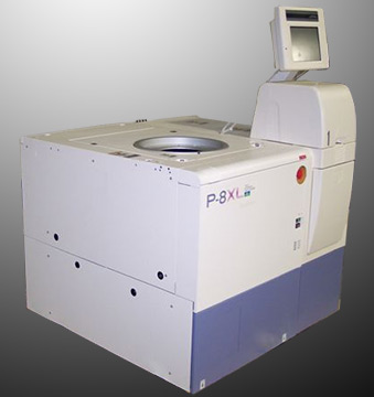
Tokyo Electron Ltd (TEL) P8 & P8XL Map Format

These probers output a pair of binary files containing the wafer map data.

p8xl.jpg

LOT.DAT

This is a small binary file that stores lot information, wafer parameters and other data. The actual map data is not contained in this file.


W-NO-xx.DAT

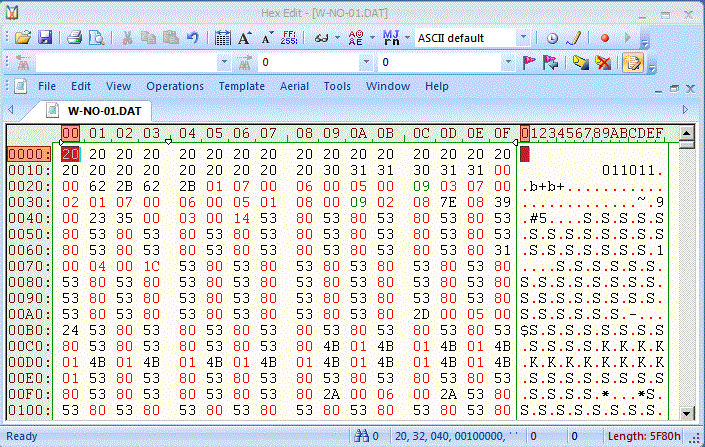
This binary file stores the wafer map data based on the results of the probing. Each file has the map for a single wafer and up to 50 wafer files can be created for each LOT.DAT file.

p8_wafer.dat.gif

Since the wafer.dat file is binary, it is not man-readable. A program must be written to extract the map data and convert it to some sort of ASCII/XML format.

Once you pass the header section, the balance of the file consists of map data. Each device or bin uses 2 Bytes.

Variations?

It is possible that there are some variations in the binary files output by different versions of this machine. We have seen two different documentation for the header part of the WAFER-XX.DAT file.


Additional Formats

Our understanding is that there are hundreds of different wafer map formats out there. We can add support for more formats as they are made available to us. If you have a format you need supported please contact:


Steve DiBartolomeo
Applications Manager
Steve DiBartolomeo


Download Revision History Video Tutorials Price