
 |
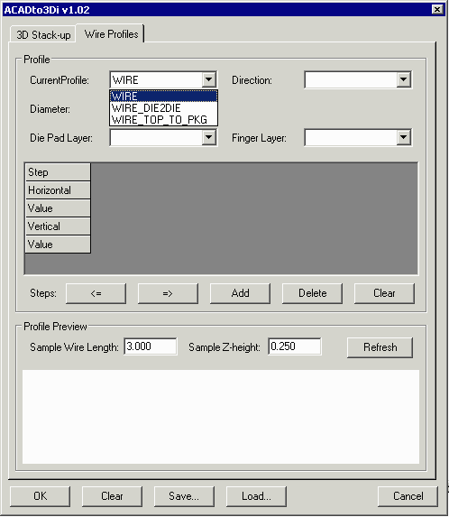
Defining Wire ProfilesNow that we have finished with the substrate and die, we need to assign profiles to our wires so that they can be modeled in 3D. For each AutoCAD layer defined as a WIRE we need to define a profile using the this tab. You can see that for this example we have three WIRE layers: WIRE, WIRE_DIE2DIE and WIRE_TOP_TO_PKG. We'll start with WIRE and use the ADD button to create a profile for it. |
|
|
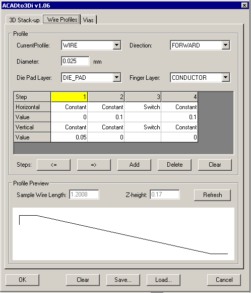
WIRE Profile The layer WIRE contains wires going from the lower die (DIE_PAD) to the fingers on layer CONDUCTOR. These wires vary in length from about 1 to 2 mm. I have created a simple custom model. The first wire motion is vertical -- 0.05 mm. The second wire step is horizontal 0.1 mm. After that, I switch sides and then tell the profile to use an 0.1 horizontal (as measured from wire end) This serves to simulate the wire foot. One can get a feel for the profile by entering some reasonable values for the Z height (vertical distance between die pad and bond finger) and the wire length. Entering 0.12 and 0.17 mm respectively and clicking on REFRESH shows the cross section. |
|
|
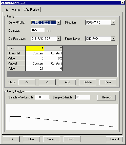
DIE2DIE Profile The layer WIRE_DIE2DIE which connects the top die to the bottom die is also very simple and uses a single vertical rise and a single horizontal motion. |
|
|
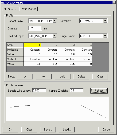
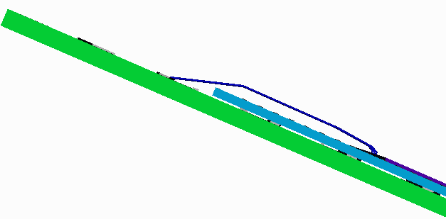
WIRE TOP_TO_PKG Profile The profile for these wires is more complicated. These wires have to fly a long distance over the bottom die and they should not drop down in a way that will hit the lower die nor should they interfere with existing wires. Therefore we used a multi-step model where the wire is formed into an arc and travels horizontally quite a distance before dropping down to the package fingers. |
|
|
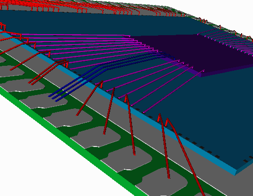
3D Results You can see a snapshot (from 3DVU) of the resulting package in 3D. One might question whether the wires from TOP_TO_PKG are touching the lower die? There are two ways to tell. Rotate the view until you can see more clearly or run a DRC within 3DVU. |
|
||
|
|||
| More Info 1 | 2 | 3 | 4 | |
| Drawing Rules | Examples | Download | Price | Revision History |
|
|