Step and Repeat Parameters
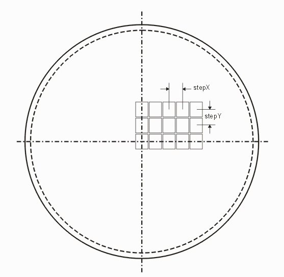
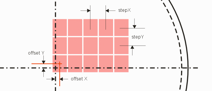
The chip foundry that made the wafer provides the stepping information in several different ways. If the wafer has only a single die on it you might get the step size for the die and generally some kind of an offset referenced to the center point of the die.

The entire array of die can also be "offset" - this is measured from the center of the die to the center of the wafer.

Potential Errors?
A user who relies on a GDSII layout tool must manually place the die and then create insertions based on the stepping size. The first die must be correctly shifted. Finally the user will need to manually delete any die that fall outside the extents of the round wafer. A large wafer with a small die could easily hold 7000 devices. This is very time consuming. An automated program such as GDS-SR can generate a properly clipped array of devices and return a count in only a few seconds.
Reticle Input?
Foundries rarely provide the stepping data in such a straightforward manner. This is because they don't actually place the die on the wafer individually. Instead they have a reticle mask that contains a number of die. It is the reticle that is stepped across the wafer. The number of die that are placed on a reticle varies - depending mostly on the die size. We'll show how to handle reticle input on the next page.
