Preparing a Flip Chip Mask Set
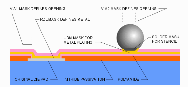
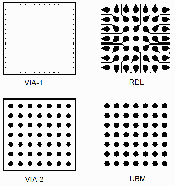
Converting a "conventional" wirebond die into a flip chip die generally requires that a series of back end steps are performed on a full sized wafer. This normally requires a set of 4 masks on large glass plates (10 inch for 200 mm wafers and 14-15 inches for 300 mm wafers.)

These masks include the following:
VIA-1 - used to expose the original die pads after a polyamide layer has been spun over the wafer.
RDL - (redistribution layer) used to define metal traces from the original die pads to the new locations for the bumps. Note that the RDL metal is applied initially by sputtering and then is plated up to the desired thickness.
VIA-2 used to create openings in the dielectric over the RDL metal
UBM - (under bump metal) used to define and plate up metal connecting the RDL layer to the bump.
SOLDER - used to produce a screen or stencil through which solder is applied to the under bump metal. The round solder bumps will adhere to this solder. You don't need an expensive glass mask for this -- a film mask will be sufficient.

