Plated Layers Need Constant Density ...
Two of the masks we are preparing involve plating -- the RDL mask and the UBM mask. In both cases the mask defines areas where metal will be deposited and plated up. The very first thin layer of metal is applied by sputtering -- but the sputtering process builds up the metal very slowly so it is only used to put a very thin layer down. Then more metal is applied by plating over the sputtered layer.
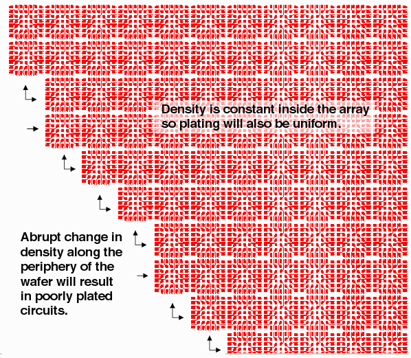
You could say that plating is both a chemical and a physical process. It turns out the the rate of plating of any particular location depends on the density of the plating chemicals and the density of the electrical current. These are both affected by the local density of the metal being plated.
If you have abrupt changes in metal density, you will get non-uniform plating and this can adversely affect the yield of your circuits.
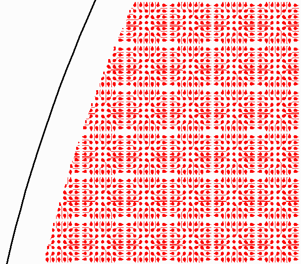
The bottom line is that one has to maintain the metal density over the "good" cells or you may lose them due to poor plating.
|


