Hextract Web Page Header


The Unit Cell Design

The Wafer/Die Settings

Matching Existing Die

Generating the Array
with GDS-SR

Plating on RDL/UBM

Clip to a Round Boundary

Knocking Out Openings

Dropping in the FIDS

Solder Stencil Issues


Stepping to Match the Wafer

Since a wafer has already been built, we need to array our unit cell to exactly match the array of die on the wafer. This requires both a) that we use the correct step size and b) that we shift or offset our array so that it matches the how the original die was stepped.

Normally this information is provided by the fab that built the wafer. However it may be provided in a way that requires some analysis or massaging to be usefult to the flip chip mask designer. Most fabs use a reticle and you may get the reticle flash locations. You will then need to know more about the die's location on the reticle in order to find the center and extents of the array.

The fab should also supply some coordinates (with respect to the center of the wafer) that tell you where test devices are located and where a wafer ID and fiducials are located. We will need this information to knockout regions of our Flip Chip masks so that these locations can be accessed or viewed.
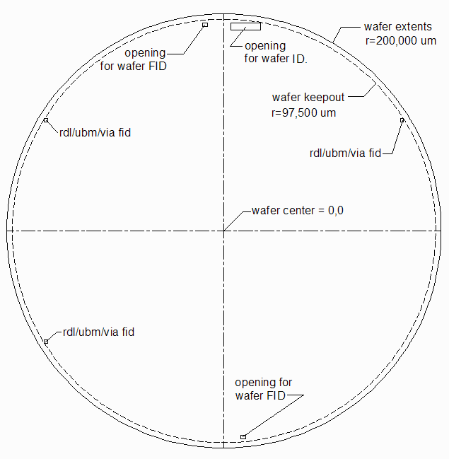
wafer layout with FIDs and Openings for Wafer ID


Getting the Array Aligned

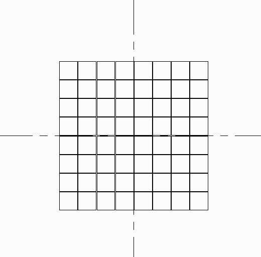
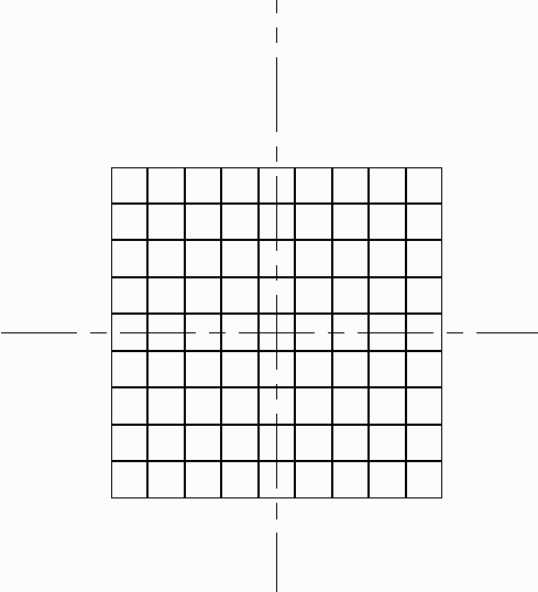
Generally there is no problem getting the die stepping information in terms of the X and Y stepping distance. However getting information about how the array is "centered" on the wafer is another matter. There are three options:

    (a) The array is die centered

    (b) The array is street centered

    (c) The array is neither die nor street centered


street centered array

street centered array


die centered array

die centered array


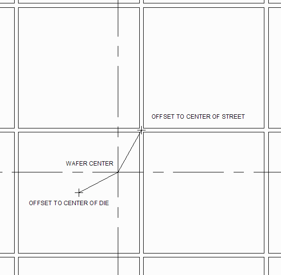
If the array of die on the wafer was neither street centered nor die centered then the fab will have to provide you a diagram of the offset of the center of the array with respect to the center of the wafer. It is very important to get this right and it may be worthwhile, prior to making a glass mask, to create a film mask which is very cheap showing the array outlines and cutouts and physically checking against a completed wafer.


offset centered array

offset centered array - the fab should provide distance from die center or street center to the center of the wafer ....


NEXT Using GDS_SR to step out the array ...


  Download   Application Note   Revision History   Price